MCPCB for Solar Inverters: Thermal Performance in Renewable Energy Systems
Metal Core Printed Circuit Boards (MCPCBs) have become essential components in solar inverter designs, where efficient heat dissipation directly impacts system reliability, conversion efficiency, and operational lifespan. This technical guide explains how MCPCB thermal management capabilities address the unique challenges of renewable energy power electronics, covering material selection, design rules, and DFM considerations for solar inverter applications.
Table of Contents
- Why Thermal Management Defines Solar Inverter Reliability
- MCPCB Structure and Thermal Performance Parameters
- Material Selection for Solar Inverter MCPCBs
- Critical Design Rules for High-Power MCPCB Applications
- DFM Considerations and Common Manufacturability Pitfalls
- Thermal Testing and Performance Validation
- FAQ
- Conclusion and Design Recommendations
1. Why Thermal Management Defines Solar Inverter Reliability
Solar inverters convert DC power from photovoltaic panels into AC power for grid connection or local consumption. The power conversion stage generates significant heat, primarily from switching transistors (IGBTs or MOSFETs), rectifier diodes, and gate driver circuits. In typical residential inverters (3–10 kW), power semiconductors can dissipate 50–150 W per device. For commercial and utility-scale inverters (50 kW to several MW), thermal loads increase proportionally.
Poor thermal management leads to three critical failure modes in solar inverters. First, junction temperature rise reduces semiconductor switching efficiency and increases conduction losses, creating a thermal runaway condition. Second, thermal cycling from daily solar irradiance variations causes solder joint fatigue and delamination between the copper layer and dielectric. Third, sustained high operating temperatures accelerate electrolytic capacitor aging and reduce the mean time between failures (MTBF) of the entire inverter system.
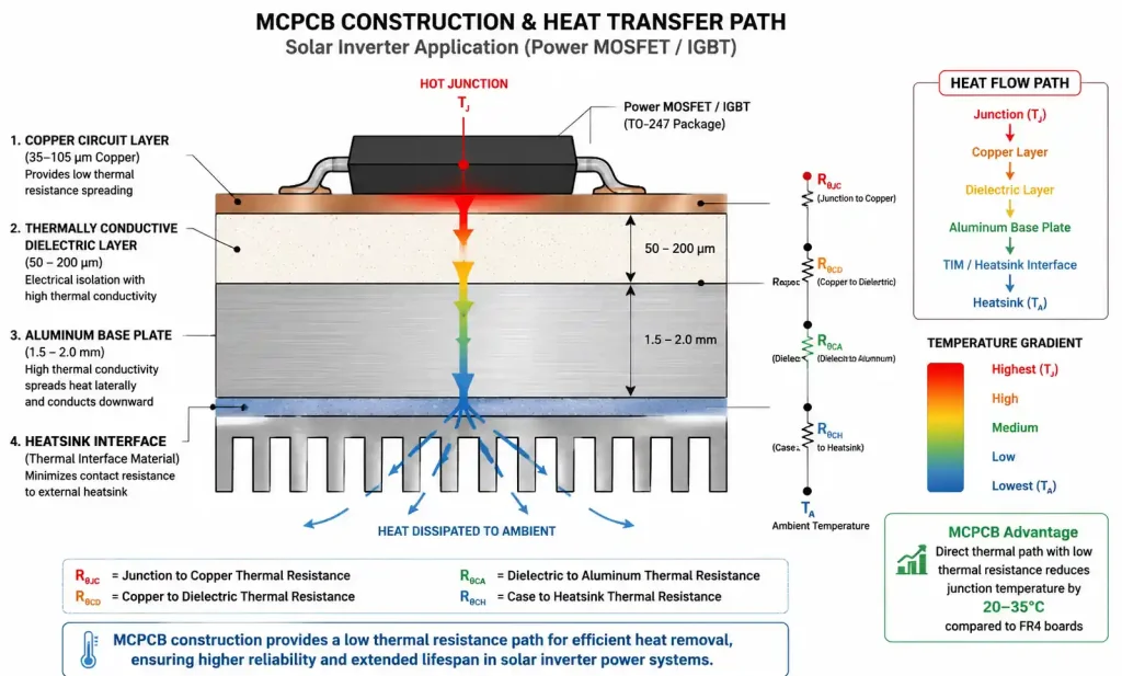
MCPCBs solve these challenges through their metal substrate layer, which provides a direct thermal path from heat-generating components to an external heatsink or cooling system. Unlike standard FR4 boards with thermal conductivity around 0.3–0.4 W/mK, MCPCB aluminum substrates typically offer 1.0–2.0 W/mK for the complete board assembly, with some high-performance dielectric materials reaching effective thermal conductivity up to 3.0–6.0 W/mK through the insulation layer.
For solar inverter design engineers, the key performance metric is junction-to-case thermal resistance (Rθ JC) combined with case-to-heatsink thermal resistance (Rθ CH). MCPCB design directly influences Rθ CH by minimizing thermal interface resistance. A well-designed MCPCB for a 100 A IGBT module can reduce component junction temperature by 20–35°C compared to FR4 boards with thermal vias, extending device lifetime by 2–5× according to Arrhenius reliability models.
2. MCPCB Structure and Thermal Performance Parameters
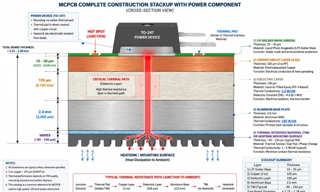
A typical MCPCB consists of four layers: copper circuit layer, thermally conductive dielectric layer, metal base (usually aluminum or copper), and optional solder mask. The dielectric layer is the critical thermal interface, as it must provide both electrical insulation (typically 3–4 kV breakdown voltage) and low thermal resistance.
The effective thermal performance of an MCPCB depends on three material parameters: dielectric thermal conductivity (λ d), dielectric thickness (t d), and copper layer thickness (t cu). The thermal resistance through the dielectric layer can be approximated as R θ = t d / (λ d × A), where A is the contact area. For solar inverter power stages, engineers typically target dielectric thermal resistance below 1.0°C/W for TO-247 package footprints and below 0.5°C/W for larger power modules.
Table 1: MCPCB Layer Structure and Typical Parameters for Solar Inverter Applications
| Layer | Material Options | Thickness Range | Thermal Conductivity | Purpose |
|---|---|---|---|---|
| Circuit layer | 1–4 oz copper | 35–140 μm | 385 W/mK | Current carrying, component mounting |
| Dielectric | Epoxy resin, polyimide, ceramic-filled | 50–200 μm | 1.0–6.0 W/mK | Electrical isolation, thermal transfer |
| Metal base | Aluminum 5052/6061, copper | 1.0–3.0 mm | Al: 120–200 W/mK, Cu: 385 W/mK | Heat spreading, mechanical support |
| Solder mask | LPI, TPSR | 15–30 μm | 0.2–0.3 W/mK | Component protection, not on thermal pads |
The metal base thickness affects heat spreading rather than direct thermal transfer. For solar inverters with multiple power devices distributed across the board, a thicker aluminum base (1.5–2.0 mm) provides better lateral heat spreading, reducing hot spots. However, thicker substrates increase material cost and board weight, which matters for rooftop residential installations.
Copper circuit layer thickness directly impacts current carrying capacity. Solar inverter power stages with 50–100 A DC bus currents typically require 3–4 oz copper (105–140 μm). The relationship between copper thickness, trace width, and allowable temperature rise follows IPC-2152 guidelines, but MCPCB designs can tolerate higher current densities because the metal substrate actively cools the copper traces. For example, a 5 mm wide trace with 3 oz copper on MCPCB can safely carry 40–50 A with 20°C rise, compared to 25–30 A on FR4.
3. Material Selection for Solar Inverter MCPCBs
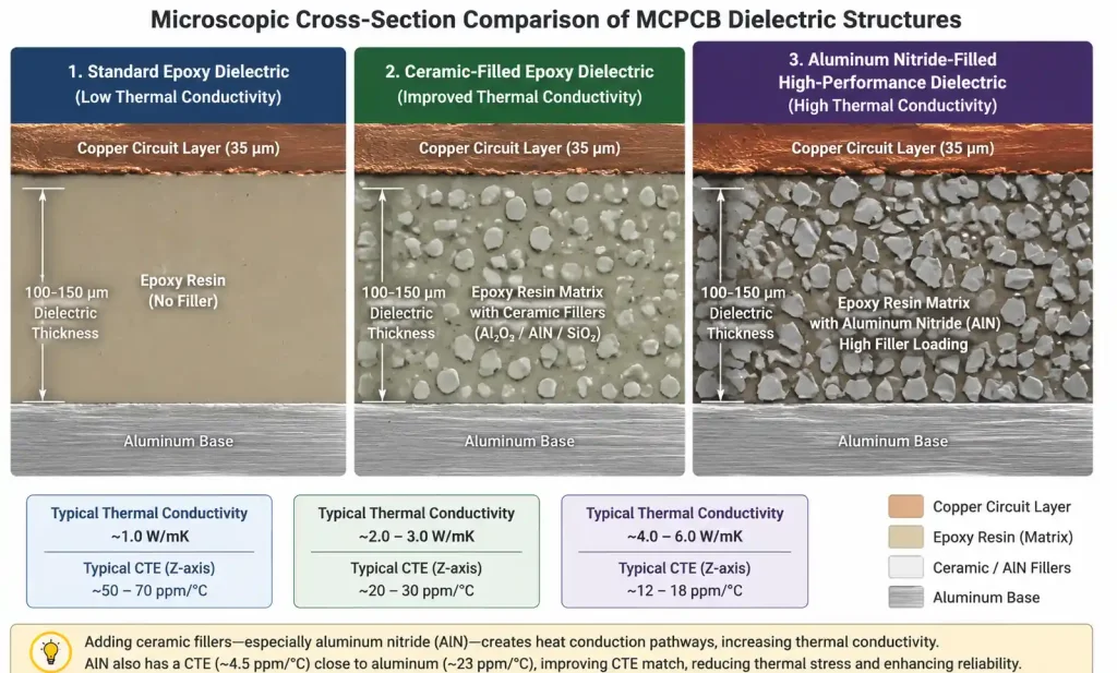
The dielectric layer material determines both thermal performance and long-term reliability under thermal cycling. Solar inverters experience daily temperature swings from ambient to 70–85°C during peak generation, then cooling overnight. This thermal cycling continues for 20–25 years of expected service life, equivalent to 7,000–9,000 cycles.
Table 2: Dielectric Material Comparison for Solar Inverter MCPCBs
| Material Type | Thermal Conductivity | Breakdown Voltage | TG (Glass Transition) | CTE Match to Al | Recommended Application |
|---|---|---|---|---|---|
| Standard epoxy | 1.0–1.5 W/mK | 3.0 kV | 130–150°C | Poor | Low-cost residential inverters <5 kW |
| High-TG epoxy | 1.5–2.0 W/mK | 3.5 kV | 170–180°C | Moderate | Mid-range commercial inverters 10–50 kW |
| Ceramic-filled epoxy | 2.0–3.0 W/mK | 4.0 kV | 180–200°C | Good | High-reliability utility-scale inverters |
| Polyimide-based | 2.5–4.0 W/mK | 4.5 kV | >250°C | Excellent | High-temperature applications, >150°C ambient |
| Aluminum nitride (AlN) | 5.0–6.0 W/mK | 5.0 kV | Not applicable | Very good | Ultra-high-power modules, >200 W/device |
For most solar inverter designs, ceramic-filled epoxy dielectrics with 2.0–3.0 W/mK thermal conductivity provide the best balance between thermal performance, reliability, and cost. The ceramic filler particles (often aluminum oxide or boron nitride) improve thermal conductivity while raising the glass transition temperature above 180°C, ensuring the dielectric remains mechanically stable during solder reflow and long-term operation.
The coefficient of thermal expansion (CTE) mismatch between the dielectric and aluminum substrate causes interfacial stress during thermal cycling. Standard epoxy resins have CTE around 50–70 ppm/°C, while aluminum 6061 has CTE around 23 ppm/°C. This mismatch can lead to delamination after several thousand cycles. High-performance dielectrics use ceramic fillers to reduce CTE to 30–40 ppm/°C, significantly improving thermal cycling reliability. For solar inverters expected to last 25 years, specify dielectrics that have passed at least 1,000 cycles of -40°C to +125°C thermal shock testing per IPC-TM-650 2.6.7.
Base metal selection depends on thermal performance requirements and weight constraints. Aluminum alloy 5052 or 6061 is standard for most solar inverter applications, offering thermal conductivity around 150–200 W/mK at approximately one-third the weight and cost of copper. Copper base MCPCBs provide superior heat spreading (385 W/mK) but are typically reserved for ultra-high-power applications where the thermal benefit justifies the added weight and expense. Some designs use aluminum-copper composite bases, with a thin copper layer bonded to aluminum for improved heat spreading near concentrated thermal loads.
4. Critical Design Rules for High-Power MCPCB Applications
MCPCB design rules differ from standard PCB guidelines due to the metal substrate and the need for direct component thermal coupling. The following parameters directly impact both electrical performance and thermal management effectiveness.
Table 3: Design Rule Requirements for Solar Inverter MCPCBs (by IPC Class)
| Design Parameter | IPC Class 2 (Industrial) | IPC Class 3 (High Reliability) | Solar Inverter Typical |
|---|---|---|---|
| Minimum trace width (3 oz Cu) | 0.3 mm | 0.4 mm | 0.5 mm (power), 0.2 mm (signal) |
| Minimum trace spacing | 0.3 mm | 0.4 mm | 0.5 mm (>50 V), 0.3 mm (<50 V) |
| Minimum via diameter | 0.3 mm | 0.4 mm | 0.6 mm (thermal vias in Cu layer) |
| Minimum annular ring | 0.1 mm | 0.15 mm | 0.15 mm |
| Clearance to board edge | 2.0 mm | 2.5 mm | 3.0 mm (to prevent Al substrate exposure) |
| Solder mask clearance on thermal pads | N/A | N/A | No solder mask (direct component contact) |
| Copper to dielectric overlap | 0.5 mm | 0.5 mm | 0.8 mm (prevents edge shorting to Al base) |
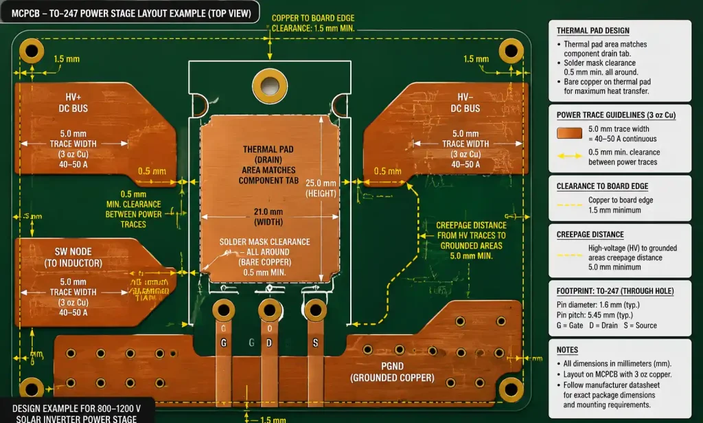
Thermal pad design is critical for power semiconductors. The component thermal pad must make direct contact with the copper circuit layer, which then transfers heat through the dielectric to the aluminum substrate. Solder mask must not be applied over thermal pads, as even a thin 25 μm solder mask layer adds significant thermal resistance. For TO-220, TO-247, and power module packages, create a bare copper thermal pad that matches or slightly exceeds the component’s thermal tab area.
Copper trace current carrying capacity on MCPCB follows modified IPC-2152 calculations. Because the metal substrate actively cools the copper layer, MCPCBs can handle higher current densities than FR4 boards. For a 10°C temperature rise with 3 oz copper on aluminum MCPCB, use these approximate current capacities: 1 mm trace width carries 8–10 A, 3 mm carries 20–25 A, 5 mm carries 40–50 A. These values assume good thermal coupling through a dielectric with 2.0 W/mK thermal conductivity and adequate heatsink design.
Creepage and clearance requirements for solar inverter designs must comply with safety standards including UL 1741, IEC 62109, and EN 50178. For DC bus voltages up to 1000 V (typical for residential string inverters), maintain minimum 5 mm creepage distance between high-voltage conductors and grounded metal substrate. For voltages above 1000 V (common in commercial three-phase systems), increase creepage to 8–10 mm. The MCPCB manufacturing process must ensure the aluminum substrate is properly isolated, with the copper circuit layer stopping at least 0.8–1.0 mm from the board edge to prevent accidental shorting to the exposed metal base.
Via design on MCPCBs differs from standard PCBs because vias penetrate only the copper circuit layer, not through to the aluminum base. These blind vias connect signal traces but do not provide thermal pathways. For thermal management, the primary heat transfer path is through the dielectric layer directly under power components, not through vias. If multilayer signal routing is needed, specify a double-sided MCPCB with a thin FR4 or polyimide insulation layer between two copper circuit layers, though this construction increases cost and thermal resistance.
5. DFM Considerations and Common Manufacturability Pitfalls
MCPCB manufacturing involves unique processes that differ from standard PCB fabrication, particularly in drilling, routing, and surface finish application. Understanding these manufacturing constraints prevents costly design respins and production delays.
Table 4: MCPCB DFM Checklist for Solar Inverter Applications
| Design Element | DFM Requirement | Risk if Violated | Recommended Practice |
|---|---|---|---|
| Copper to board edge | ≥ 1.0 mm clearance | Short circuit to Al substrate | Use 1.5 mm as standard clearance |
| Thermal pad size | Match component thermal tab ± 0.5 mm | Poor thermal contact or solder bridging | Exact match preferred, slight overhang acceptable |
| Solder mask on thermal areas | Prohibited | Thermal resistance increase 0.5–1.0°C/W | Specify “no solder mask” on thermal pads |
| Drilling into Al base | Avoid unless mounting holes | Drill bit breakage, burr formation | Use controlled depth routing for circuit features |
| V-cut or routing depth | Set to copper + dielectric thickness only | Damage to Al base, routing tool wear | Specify partial depth, leave Al intact |
| Minimum hole diameter | 0.8 mm for through-holes | Difficulty drilling composite materials | Use 1.0 mm or larger when possible |
The most common DFM error in MCPCB designs is allowing copper traces or pads to extend too close to the board edge. During CNC routing or V-cut depaneling, if copper is closer than 1.0 mm to the edge, there is risk of copper delamination or accidental exposure of the aluminum substrate, creating a potential short circuit. Always maintain at least 1.5 mm clearance from copper features to the final board edge.
Thermal pad design requires careful coordination with component package specifications. For power MOSFETs in D2PAK or DPAK packages, the thermal pad on the PCB should match the component’s exposed drain pad within ±0.3 mm. If the PCB thermal pad is too small, thermal contact area decreases and thermal resistance increases. If the pad is significantly oversized, excess solder can wick out during reflow, creating voids under the component. For large power modules with multiple thermal tabs, create separate thermal pads for each tab rather than one large continuous pad, as this improves solder joint inspection and reduces voiding.
Surface finish selection impacts both solderability and thermal performance. ENIG (Electroless Nickel Immersion Gold) is common for MCPCBs because it provides good solderability and multiple reflow capability, but the nickel layer (typically 3–5 μm) adds slight thermal resistance. For maximum thermal performance on high-power pads, specify immersion silver or OSP (Organic Solderability Preservative) finish, which adds minimal thermal resistance. However, OSP has limited shelf life (6 months) and single reflow capability, so it is best suited for high-volume production with short lead times.
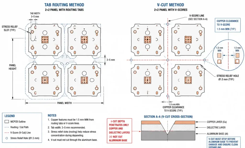
Panelization and depaneling of MCPCBs requires special consideration due to the metal substrate. V-cut scoring is possible but must be set to cut only through the copper and dielectric layers, stopping before the aluminum base. The aluminum is then broken along the V-cut line during depaneling. Tab routing is generally preferred, where small tabs connect individual boards within a panel, and these tabs are routed through the full board thickness including aluminum. After assembly, the tabs are broken or cut to separate individual boards. For solar inverter PCBs with high-power components, minimize mechanical stress during depaneling by using tab routing with stress relief slots rather than V-cut.
6. Thermal Testing and Performance Validation
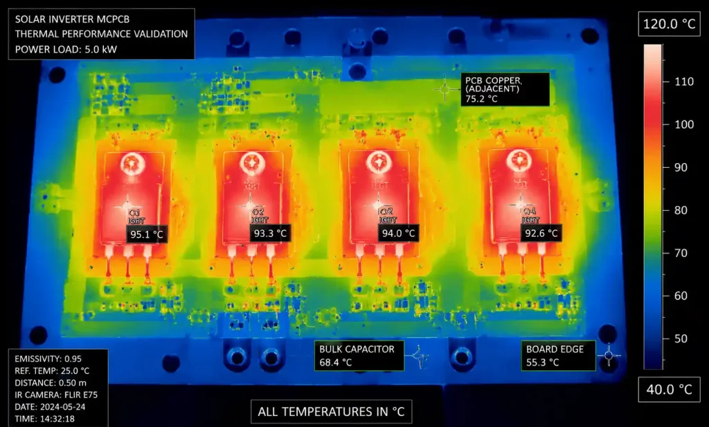
Validating MCPCB thermal performance before full production prevents field failures and ensures solar inverter reliability. Thermal testing should occur at both the board level (before assembly) and system level (after component mounting and integration with heatsinks).
Board-level thermal characterization measures the dielectric layer thermal resistance using standardized test methods. The most common approach follows ASTM D5470, where a calibrated heat source and temperature sensors measure heat flux through the MCPCB sample. For solar inverter applications, target dielectric thermal resistance below 1.0°C·cm²/W for standard designs and below 0.5°C·cm²/W for high-performance applications. This measurement should be performed on incoming material inspection to verify supplier specifications.
Component-level thermal testing uses infrared thermography or thermocouple measurements to validate junction temperatures under realistic power dissipation. For power semiconductors, apply rated current and measure case temperature at steady state, then calculate junction temperature using the device’s published thermal resistance specifications. A well-designed MCPCB for a 150 W IGBT should maintain junction temperature below 125°C with 85°C ambient and appropriate heatsink design. If measured temperatures exceed design predictions by more than 10–15°C, investigate thermal interface issues such as solder voids, insufficient thermal compound, or poor heatsink contact.
Table 5: Thermal Testing Methods and Acceptance Criteria for Solar Inverter MCPCBs
| Test Method | Purpose | Equipment | Acceptance Criteria | Frequency |
|---|---|---|---|---|
| ASTM D5470 thermal resistance | Verify dielectric thermal performance | Guarded heat flow meter | < 1.0°C·cm²/W for standard, < 0.5°C·cm²/W for high-performance | First article, material change |
| IR thermography | Identify hot spots and thermal distribution | Thermal imaging camera | No hot spots > 10°C above design prediction | Prototype validation, design verification |
| Thermocouple measurement | Validate component junction temperature | K-type thermocouples, data logger | Tjunction < 125°C at rated power with 85°C ambient | Every design revision |
| Thermal cycling (IPC-TM-650 2.6.7) | Assess solder joint and delamination reliability | Thermal chamber | No delamination or cracking after 1000 cycles (-40 to +125°C) | First article, qualification |
| Power cycling (JEDEC JESD22-A122) | Simulate real-world thermal stress | Power supply, thermal chamber | No failures before 10,000 cycles (ΔT = 80°C) | New product qualification |
Thermal cycling and power cycling tests simulate long-term reliability under temperature stress. Solar inverters experience daily power cycling as solar irradiance varies from morning to peak to evening, creating thermal stress on solder joints and the dielectric-to-metal interface. Accelerated thermal cycling per IPC-TM-650 method 2.6.7 (typically 1,000 cycles from -40°C to +125°C with 15-minute dwell times) screens for delamination and CTE mismatch issues. For critical applications, extend testing to 2,000–3,000 cycles to better represent 20–25 year field life.
Power cycling per JEDEC JESD22-A122 applies realistic electrical load cycling, turning power semiconductors on and off to create junction temperature swings of 80–100°C. This test stresses solder joints between component thermal pads and the MCPCB copper layer. Target at least 10,000 power cycles without solder joint cracking or thermal resistance increase for commercial solar inverter applications. Utility-scale inverters with 25+ year design life should demonstrate 25,000–50,000 cycle capability.
7. FAQ
What is the typical thermal conductivity range for MCPCB dielectrics used in solar inverters?
MCPCB dielectric thermal conductivity ranges from 1.0 W/mK for standard epoxy formulations to 6.0 W/mK for advanced aluminum nitride filled materials. For most solar inverter applications, ceramic-filled epoxy with 2.0–3.0 W/mK provides the best balance of thermal performance, electrical insulation, and cost. This level supports power dissipation up to 100–150 W per device with appropriate heatsink design.
How much temperature reduction can MCPCB provide compared to FR4 for power electronics?
Compared to FR4 PCBs with thermal vias, a well-designed MCPCB can reduce component junction temperatures by 20–35°C under the same power dissipation and heatsink conditions. This temperature reduction directly translates to 2–5× longer component life based on semiconductor reliability models. The exact improvement depends on dielectric thermal conductivity, base metal thickness, and thermal interface design.
Can I use standard PCB assembly equipment for MCPCB boards?
Yes, MCPCBs are compatible with standard SMT assembly equipment including solder paste printing, pick-and-place, and reflow ovens. However, heavier aluminum substrates (2–3 mm thick) may require fixture adjustments to support board weight during transport. Reflow profiles should be optimized for MCPCB thermal mass, typically extending preheat time by 20–30 seconds compared to FR4 boards of similar size.
What clearance distance is required between copper traces and the aluminum substrate edge?
Maintain minimum 1.0 mm clearance between any copper features and the final board edge to prevent accidental shorting to the aluminum substrate. For production reliability, 1.5 mm clearance is recommended as standard practice. This clearance accounts for routing tolerance and copper edge delamination during depaneling.
How does MCPCB thickness affect thermal performance?
Total MCPCB thickness primarily affects heat spreading, not direct thermal transfer. The dielectric layer thickness (typically 50–200 μm) controls thermal resistance from copper to aluminum. Thicker aluminum substrates (1.5–3.0 mm) improve lateral heat spreading for distributed power components but add weight and cost. For concentrated thermal loads under a single component, dielectric thickness is more important than aluminum thickness.
Are there special design rules for high-voltage solar inverter applications?
Yes. For DC bus voltages up to 1000 V, maintain minimum 5 mm creepage distance between high-voltage traces and the aluminum substrate or ground planes. For voltages above 1000 V, increase creepage to 8–10 mm per IEC 62109 requirements. Ensure copper circuit layer stops at least 1.0 mm from board edges to prevent high-voltage exposure to the metal substrate.
What surface finish is best for MCPCB thermal pads?
For maximum thermal performance, use immersion silver or OSP on thermal pads, as these finishes add minimal thermal resistance. ENIG is acceptable for general use but the 3–5 μm nickel layer slightly increases thermal resistance. Avoid HASL on thermal pads as the thick solder layer creates uneven surfaces that reduce component thermal contact area.
How should I specify panelization for MCPCB manufacturing?
Tab routing is generally preferred over V-cut for MCPCBs because it provides cleaner separation without stress concentration. If V-cut is used, specify scoring depth to penetrate copper and dielectric layers only, stopping before the aluminum base. Include stress relief holes (typically 1.5 mm diameter) at V-cut intersections to facilitate clean breaking without aluminum deformation.
8. Conclusion and Design Recommendations
MCPCB technology is essential for solar inverter designs that prioritize thermal management, long-term reliability, and power conversion efficiency. The metal core substrate provides direct thermal pathways that reduce component junction temperatures by 20–35°C compared to FR4 alternatives, directly extending semiconductor lifespan and improving inverter reliability over 20–25 year service life.
For solar inverter design engineers, prioritize these key parameters: select ceramic-filled epoxy dielectrics with thermal conductivity of 2.0–3.0 W/mK for the best balance of performance and cost; specify 3–4 oz copper circuit layers for high current capacity; maintain proper creepage distances (5 mm minimum for systems up to 1000 V); and ensure thermal pads are free of solder mask for direct component thermal contact.
For power electronics applications with sustained thermal loads above 100 W per device, conduct thorough thermal testing including IR thermography and power cycling validation before volume production. Verify that junction temperatures remain below 125°C at maximum ambient conditions and that the design survives at least 10,000 thermal cycles without delamination or solder joint failure.
Before submitting Gerber files for manufacturing, review the DFM checklist: confirm all copper features maintain 1.5 mm clearance from board edges, verify thermal pad dimensions match component specifications, specify no solder mask on thermal areas, and select appropriate surface finish (immersion silver or OSP preferred for thermal pads). For assistance with MCPCB design review or thermal simulation analysis, consult with your PCB manufacturer’s engineering team early in the design cycle to optimize layer stackup and material selection for your specific power dissipation requirements.