
Achieving Length Matching in PCB Design: Techniques and Best Practices
Introduction
In modern high-speed printed circuit board (PCB) design, signal integrity has become a critical factor affecting system performance. One of the most important aspects of maintaining signal integrity is implementing proper length matching (also called equal length routing) for critical signal traces. This article provides a comprehensive guide to achieving precise length matching in PCB design, covering fundamental concepts, implementation techniques, and practical considerations.
Understanding the Need for Length Matching
Why Length Matching Matters
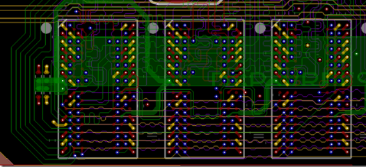
In high-speed digital systems and differential pair signaling, signals often need to arrive at their destinations simultaneously or within precise timing relationships. When signals in a bus or differential pair travel different distances, they experience different propagation delays, leading to:
- Skew: Timing differences between related signals
- Phase mismatches: In differential signaling, causing common-mode noise
- Reduced timing margins: Potentially leading to setup/hold time violations
- Signal integrity degradation: Increased jitter and reduced eye diagram quality
When Length Matching is Required
Common scenarios requiring length matching include:
- DDR memory interfaces (address/command/control buses, data lanes)
- Differential pairs (USB, HDMI, PCI Express, Ethernet)
- High-speed parallel buses
- Clock distribution networks
- Any synchronous interface where timing relationships are critical
Fundamental Concepts
Propagation Velocity and Delay
The propagation delay of a signal in a PCB trace depends on:
- The dielectric constant (Dk or εr) of the PCB material
- The trace geometry (microstrip or stripline)
- The signal frequency (due to dispersion effects)
The delay is typically expressed as ps/inch or ps/mm. For FR4 material (εr ≈ 4.2-4.5):
- Microstrip: ~140-170 ps/inch
- Stripline: ~170-180 ps/inch
Length Matching Tolerance
The acceptable length mismatch depends on:
- The signal rise/fall time (faster edges require tighter matching)
- The clock frequency (higher frequencies require tighter matching)
- The interface specifications (e.g., DDR standards specify maximum skew)
Typical requirements:
- DDR4/5: ±50 mils (1.27mm) for address/command, ±5 mils (0.127mm) for clocks
- USB 3.0: ±50 mils differential pair matching
- PCIe Gen3: ±5 mils within a pair, ±500 mils between pairs
PCB Stackup Considerations
Proper stackup design is foundational for successful length matching:
- Controlled impedance: Ensure consistent impedance for all matched traces
- Symmetrical layer stacking: Minimizes variations in dielectric properties
- Reference planes: Provide solid return paths for high-speed signals
- Dielectric material selection: Low-loss materials (e.g., Rogers) for very high speeds
Length Matching Techniques
1. Topological Planning
Before routing begins:
- Group related signals: Keep matched nets physically close
- Plan routing paths: Determine common routing areas and detour regions
- Identify matching groups: Classify nets by their matching requirements
2. Basic Routing Approaches
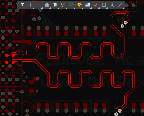
A. Serpentine Routing (Trombone/Tuning Meanders)
The most common technique for adding length to shorter traces:
- Single-sided serpentines: All bends on one side
- Double-sided serpentines: Bends alternating on both sides
- Sawtooth patterns: Angled segments instead of right angles
Best practices:
- Maintain consistent spacing between meander segments (≥3× trace width)
- Use gradual bends (45° or curved) rather than 90° angles
- Keep meander sections away from vias and component pads
B. Spiral Routing
For cases requiring significant length addition:
- Compact circular or rectangular spirals
- Useful when space is limited in one dimension
C. Differential Pair Length Matching
Special considerations for differential pairs:
- Match lengths within the pair first
- Then match the pair to other pairs as needed
- Maintain consistent spacing throughout the pair
3. Advanced Techniques
A. 3D Length Matching
For multi-layer designs:
- Account for via stub effects
- Match total path length including layer transitions
- Consider using back-drilled or blind vias for critical signals
B. Delay Matching (vs. Pure Length Matching)
In some cases, electrical length matters more than physical length:
- Adjust for different propagation speeds on different layers
- Consider dielectric constant variations
- May require length adjustments based on simulation
C. Dynamic Phase Matching
For very high-speed designs (e.g., >10Gbps):
- Match phase delays rather than simple lengths
- Requires electromagnetic simulation
- May involve intentional length mismatches to compensate for other effects
Implementation in PCB Design Tools
Modern EDA tools offer powerful features for length matching:
1. Constraint Management
- Set up matching groups and tolerances
- Define relative vs. absolute matching requirements
- Specify different rules for different net classes
2. Interactive Length Tuning
- Real-time length calculation during routing
- Visual feedback (color coding, length indicators)
- Automated meander insertion
3. Post-Route Verification
- Length matching reports
- 3D electromagnetic analysis
- Signal integrity simulation
4. Automated Optimization
Some advanced tools offer:
- Automatic length matching during routing
- Batch processing of matching groups
- Intelligent meander pattern generation
Practical Challenges and Solutions
1. Space Constraints
Solutions:
- Use higher density meander patterns where space is limited
- Distribute length matching across multiple routing areas
- Consider layer changes to access more routing space
2. Crosstalk Concerns
Mitigation strategies:
- Increase spacing between meander sections and other traces
- Use ground guards between sensitive traces
- Avoid parallel runs of matched traces over long distances
3. Manufacturability
Considerations:
- Maintain minimum bend radii for fabricator capabilities
- Ensure adequate spacing for etching tolerance
- Account for copper roughness effects at high frequencies
4. Mixed-Signal Environments
Approaches:
- Separate analog and digital matched groups
- Use different matching strategies for each domain
- Pay special attention to ground return paths
Verification and Testing
1. Design Verification
- DRC (Design Rule Checking) for physical matching
- Electrical Rule Checking (ERC) for timing constraints
- 3D electromagnetic simulation for critical paths
2. Prototype Testing
- Time-domain reflectometry (TDR) for impedance verification
- Eye diagram analysis for high-speed interfaces
- Jitter measurements to validate timing margins
Future Trends
Emerging technologies affecting length matching:
- Higher frequencies: Terahertz interconnects requiring sub-mil matching
- 3D packaging: Length matching across die, package, and board
- AI-assisted routing: Machine learning for optimal matching patterns
- Photonic interconnects: New challenges in optical path matching
Conclusion
Achieving precise length matching in PCB design requires careful planning, proper tool utilization, and attention to both electrical and physical constraints. By understanding the fundamental principles, implementing appropriate techniques, and verifying results through simulation and testing, designers can ensure robust signal integrity in high-speed digital systems. As data rates continue to increase, the importance of accurate length matching will only grow, making these skills essential for modern PCB designers.
The key to success lies in:
- Early planning of matching requirements
- Proper constraint setup in design tools
- Methodical implementation of matching techniques
- Comprehensive verification at all stages
By mastering these aspects, designers can effectively meet the challenges of length matching in increasingly complex PCB designs.