Adding x and z gaps around the PCB
1.Adding x and z gaps around the PCB
So far, all the cases we have considered have had physical contact between the edge of the PCB and the housing. Although the contact area is small, it can be seen from Figure 6 that the amount of heat transferred through this path is significant, accounting for about 20% of the total heat in the case of the black plastic housing.
However, in real conditions, some configurations may have an air gap between the edge of the PCB and the housing – perhaps to provide electrical isolation or for other purposes, such as mechanical reasons. Introducing such an air gap will change the available thermal path within the module and inevitably affect the temperature of the MOSFET device mounted on the PCB.
To investigate the effect of air gaps around the PCB, we reran the previous model, but this time with x and z gaps of 5mm and 10mm respectively. See Figure 8.
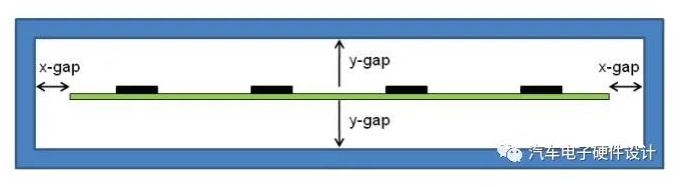
Figure 8: Gap around the PCB.
2.Black plastic housing.
The results for the black plastic housing are shown in Figure 9.
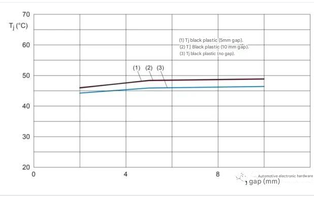
(1) Tj black plastic (5mm gap).
(2) Tj black plastic (10mm gap).
(3) Tj black plastic (no gap).
Figure 9: Effect of x-z gap on Tj of black plastic housing
Although we can see some difference when introducing the gap, it can be considered that the effect is not significant – about 2.5°C. This is because plastic material is not a good conductor of heat, so conduction into the housing is not the main heat path (see Figure 6). In addition, the increased angle factor leads to improved radiation heat transfer. Therefore, removing the conduction path does not lead to a drastic change in temperature.
3.Polished aluminum housing
It can be expected that the aluminum housing will have a more significant effect because aluminum is a better conductor of heat than plastic, so the effect of removing this conduction path on Tj should be greater. The results for the polished aluminum housing are shown in Figure 10.
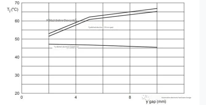
(1) Tj polished aluminum (5mm gap).
(2) Tj polished aluminum (10mm gap).
(3) Tj polished aluminum (no gap).
Figure 10: Effect of x and z gaps on Tj of polished aluminum housing
In this case, the effect of adding x and z gaps around the PCB is more pronounced, especially as the y gap is increased, which produces a difference of about 20°C when the y gap is 10mm. By removing the conduction path at the edge of the PCB, we have increased the thermal isolation between the PCB and the enclosure:
- Direct conduction between the PCB and the enclosure is eliminated.
- Heat flow through the air is still poor because the air is still stagnant.
- Radiative heat transfer is also poor because the surface emissivity of aluminum is low.
4.Anodized aluminum enclosure
For the anodized aluminum enclosure, the effect of adding x and z gaps is less pronounced. See Figure 11.
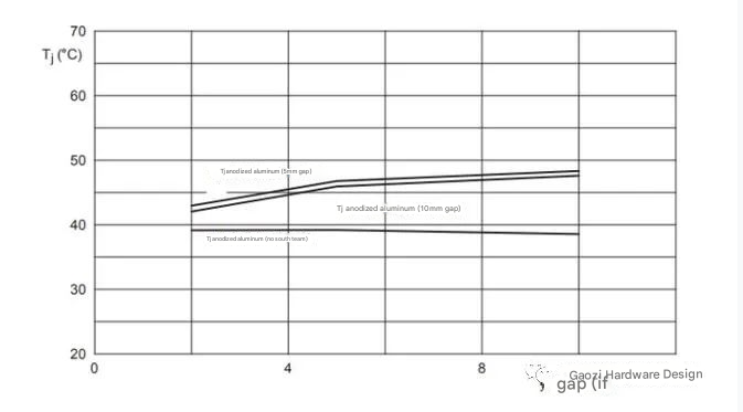
(1) Tj anodized aluminum (5mm gap).
(2) Tj anodized aluminum (10mm gap).
(3) Tj anodized aluminum (no gap).
Figure 11: Effect of x- and z-gaps on Tj for anodized aluminum enclosure
While we have lost the direct conduction heat path within the module in this example, the radiative heat path is still very effective due to the smooth surface of the enclosure material. Therefore, the change in Tj is not as large as for the polished aluminum material.
5.Summary of the three enclosure types
The results for all three enclosure types are shown in the graph of Figure 12. This graph allows us to compare the effects of the three material types when there is no direct conduction between the PCB and the enclosure.
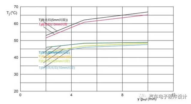
(1) Tj polished aluminum (5mm gap).
(2) Tj polished aluminum (10mm gap).
(3) Tj black plastic (5mm gap).
(4) Tj black plastic (10mm gap).
(5) Tj anodized aluminum (5mm gap).
(6) Tj anodized aluminum (10mm gap).
Figure 12. Effect of x- and z-gaps on Tj for the three enclosure materials
It should be remembered that the surface treatment of the enclosure also affects how its outer surface loses heat to the environment in the process of radiation. For example, the polished aluminum material has poorer radiative heat transfer not only between the inner surface and the PCB, but also between the outer surface and the local environment.
6. Summary: Adding x and z gaps around the PCB
l Adding a gap between the PCB and the housing eliminates the direct heat conduction path between these components;
l For the black plastic housing, the air gap does not have a large effect on Tj, since plastic is a poor thermal conductor and the radiation exchange between the surfaces is good;
l For the polished aluminum housing with a larger y-gap, the effect is more significant, since aluminum is a good thermal conductor and the radiation exchange is poor;
l The temperature change for the anodized aluminum material is somewhere between the first two sets of results. This is because, while aluminum has good thermal conductivity, the surface properties of anodized aluminum allow for good radiation heat transfer;
l Viewed side by side, the temperatures observed for the anodized aluminum and black plastic materials are fairly similar, while the polished aluminum results are higher – especially for the larger y-gap;
l The thermal conductivity and emissivity of the housing also affect the heat path through the housing and the outer surface of the housing to the surrounding environment.