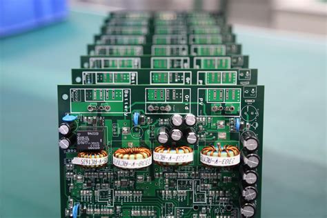
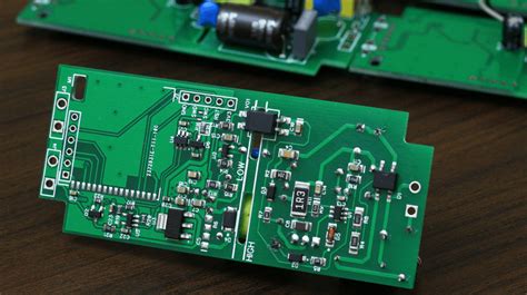
Advanced pcb design
Innovations In High-Density Interconnect (HDI) PCB Design
In recent years, the field of printed circuit board (PCB) design has witnessed significant advancements, particularly in the realm of High-Density Interconnect (HDI) technology. As electronic devices continue to shrink in size while increasing in functionality, the demand for more compact and efficient PCBs has surged. HDI technology has emerged as a pivotal solution, enabling designers to meet these demands by offering a higher wiring density per unit area compared to traditional PCBs. This innovation is primarily achieved through the use of microvias, finer lines and spaces, and advanced materials, which collectively contribute to the miniaturization and enhanced performance of electronic devices.
One of the most notable innovations in HDI PCB design is the use of microvias, which are significantly smaller than conventional vias.
These microvias allow for more interconnections in a given area, thereby increasing the routing density. By enabling connections between layers in a more compact manner, microvias facilitate the design of multi-layered PCBs without the need for additional board space. This is particularly beneficial in applications where space is at a premium, such as in smartphones, tablets, and other portable electronic devices. Furthermore, the use of microvias reduces signal loss and improves signal integrity, which is crucial for high-speed data transmission.
In addition to microvias, the development of finer lines and spaces has been instrumental in advancing HDI PCB design.
Traditional PCBs typically feature line widths and spaces that are larger, which can limit the number of connections that can be made on a single layer. However, with HDI technology, designers can achieve much finer lines and spaces, allowing for more intricate and compact circuit patterns. This not only increases the overall functionality of the PCB but also enhances its reliability by reducing the potential for electrical interference and crosstalk between adjacent traces.
The choice of materials also plays a critical role in the evolution of HDI PCB design.
Advanced materials with superior thermal and electrical properties are being utilized to support the increased density and complexity of HDI PCBs. These materials help in managing heat dissipation, which is a common challenge in densely packed electronic circuits. Moreover, they contribute to the mechanical stability of the PCB, ensuring that it can withstand the rigors of modern electronic applications. The integration of these materials into HDI PCBs has opened new avenues for innovation, enabling the development of more robust and efficient electronic devices.
As HDI technology continues to evolve, it is also driving advancements in manufacturing processes.
Techniques such as laser drilling and precision etching are being employed to create the intricate features required for HDI PCBs. These processes allow for greater accuracy and consistency, which are essential for maintaining the high standards of quality expected in modern electronics. Additionally, the adoption of automated design tools and simulation software has streamlined the design process, enabling engineers to optimize their designs for performance and manufacturability.
In conclusion, the innovations in High-Density Interconnect PCB design are reshaping the landscape of electronic device manufacturing. By leveraging microvias, finer lines and spaces, advanced materials, and cutting-edge manufacturing techniques, HDI technology is enabling the creation of smaller, more powerful, and more reliable electronic devices. As the demand for compact and efficient electronics continues to grow, HDI PCB design will undoubtedly remain at the forefront of technological advancement, driving further innovation in the industry.
Techniques For Effective Thermal Management In PCB Layouts
In the realm of advanced printed circuit board (PCB) design, effective thermal management is a critical consideration that can significantly influence the performance and reliability of electronic devices. As electronic components become increasingly powerful and compact, the challenge of dissipating heat efficiently becomes more pronounced. Therefore, understanding and implementing effective thermal management techniques in PCB layouts is essential for engineers and designers striving to optimize their designs.
One of the fundamental techniques for managing heat in PCB layouts is the strategic placement of components.
By positioning heat-generating components, such as processors and power transistors, away from heat-sensitive elements, designers can minimize the risk of thermal interference. Additionally, placing these components near the edges of the PCB can facilitate better heat dissipation, as it allows for more efficient airflow and heat transfer to the surrounding environment. This approach not only helps in maintaining the thermal integrity of the board but also enhances the overall performance of the device.
Moreover, the use of thermal vias is another effective strategy in PCB thermal management.
Thermal vias are small, plated holes that connect the top and bottom layers of a PCB, allowing heat to be conducted away from hot spots. By incorporating an array of thermal vias beneath heat-generating components, designers can create a path for heat to travel from the surface to the inner layers or to a heat sink. This technique is particularly useful in multi-layer PCBs, where heat can be distributed across different layers, thereby reducing the thermal load on any single layer.
In addition to component placement and thermal vias, the selection of appropriate materials plays a crucial role in thermal management.
High thermal conductivity materials, such as copper, are often used in PCBs to enhance heat dissipation. Copper’s excellent thermal properties make it an ideal choice for traces and planes, as it can efficiently conduct heat away from critical areas. Furthermore, incorporating thermal pads or heat sinks made from materials with high thermal conductivity can further aid in managing heat. These components can be attached to the PCB to provide additional pathways for heat to escape, thereby maintaining optimal operating temperatures.
Another technique that can be employed is the use of thermal reliefs in the design of PCB pads.
Thermal reliefs are patterns of copper that connect a pad to a plane with a reduced cross-sectional area, which helps in controlling the heat flow to and from the pad. This technique is particularly beneficial in soldering processes, as it prevents excessive heat from being conducted away from the solder joint, ensuring a reliable connection.
Furthermore, simulation tools have become indispensable in modern PCB design, allowing engineers to model and predict thermal behavior before physical prototypes are built. By using thermal simulation software, designers can identify potential hot spots and evaluate the effectiveness of various thermal management strategies. This proactive approach not only saves time and resources but also ensures that the final product meets the desired thermal performance criteria.
In conclusion, effective thermal management in PCB layouts is a multifaceted challenge that requires a combination of strategic component placement, the use of thermal vias, careful material selection, and advanced simulation techniques. By integrating these approaches, designers can create PCBs that not only perform efficiently but also maintain their reliability over time. As electronic devices continue to evolve, the importance of mastering these thermal management techniques will only grow, underscoring their significance in the field of advanced PCB design.
The Role Of Signal Integrity In Advanced PCB Design
In the realm of advanced printed circuit board (PCB) design, signal integrity plays a pivotal role in ensuring the optimal performance and reliability of electronic systems. As electronic devices become increasingly complex and compact, the demand for high-speed data transmission and minimal signal distortion has intensified. Consequently, understanding and managing signal integrity has become a critical aspect of PCB design, influencing everything from layout strategies to material selection.
Signal integrity refers to the quality and reliability of electrical signals as they travel through a PCB.
It encompasses various factors, including signal timing, amplitude, and waveform shape, all of which can be affected by the physical characteristics of the PCB. Poor signal integrity can lead to data errors, increased electromagnetic interference (EMI), and overall system instability. Therefore, maintaining signal integrity is essential for achieving the desired performance in advanced electronic applications.
One of the primary challenges in maintaining signal integrity is managing the impedance of transmission lines on the PCB.
Impedance mismatches can cause signal reflections, leading to distortion and potential data loss. To mitigate this, designers must carefully control the width, spacing, and routing of traces, as well as the dielectric properties of the materials used. By ensuring that the impedance is consistent throughout the signal path, designers can minimize reflections and maintain signal fidelity.
Moreover, the rise of high-speed digital circuits has necessitated a greater focus on minimizing crosstalk, which occurs when signals in adjacent traces interfere with each other. Crosstalk can be particularly problematic in densely packed PCBs, where space constraints make it challenging to maintain adequate separation between traces. To address this issue, designers often employ techniques such as differential signaling, which uses pairs of traces to carry signals in opposite phases, thereby canceling out interference. Additionally, careful layer stacking and the use of ground planes can help shield sensitive signals from unwanted noise.
Another critical aspect of signal integrity is the management of power distribution networks (PDNs) within the PCB.
Fluctuations in power supply can introduce noise into the system, affecting signal quality. To ensure a stable power supply, designers must optimize the placement and routing of power and ground planes, as well as incorporate decoupling capacitors to filter out high-frequency noise. By maintaining a low-impedance path for power delivery, designers can enhance signal integrity and reduce the risk of performance degradation.
Furthermore, the choice of materials plays a significant role in signal integrity.
The dielectric constant and loss tangent of the substrate material can impact signal speed and attenuation. Advanced PCBs often utilize low-loss materials to minimize signal degradation over long distances. Additionally, surface finishes and via structures must be carefully selected to reduce signal loss and maintain consistent electrical performance.
In conclusion, signal integrity is a fundamental consideration in advanced PCB design, influencing a wide range of design decisions. By addressing impedance control, crosstalk reduction, power distribution, and material selection, designers can ensure that their PCBs meet the stringent performance requirements of modern electronic systems. As technology continues to evolve, the importance of signal integrity will only grow, underscoring the need for designers to stay abreast of the latest techniques and best practices in this critical area. Through meticulous attention to detail and a comprehensive understanding of signal behavior, designers can create PCBs that deliver reliable, high-performance solutions for the most demanding applications.
Implementing Design For Manufacturability (DFM) In Complex PCBs
In the realm of advanced printed circuit board (PCB) design, implementing Design for Manufacturability (DFM) is a critical step that ensures the seamless transition from design to production, particularly in complex PCBs. As electronic devices become increasingly sophisticated, the intricacies of PCB designs have grown correspondingly, necessitating a meticulous approach to DFM. This process involves a set of guidelines and practices aimed at optimizing the design to facilitate efficient manufacturing, reduce costs, and enhance product reliability.
To begin with, one of the primary considerations in DFM for complex PCBs is the selection of materials.
The choice of substrate, copper thickness, and solder mask materials can significantly impact the manufacturability of the PCB. For instance, high-frequency applications may require specialized materials that can handle specific electrical properties, while thermal management considerations might necessitate substrates with superior heat dissipation capabilities. By carefully selecting materials that align with the intended application and manufacturing capabilities, designers can preemptively address potential production challenges.
Moreover, the layout of the PCB plays a pivotal role in DFM.
Designers must pay close attention to trace routing, component placement, and layer stack-up to ensure that the design is not only functional but also manufacturable. For example, maintaining adequate spacing between traces and components is essential to prevent short circuits and ensure signal integrity. Additionally, the strategic placement of vias and the use of blind or buried vias can help manage the complexity of multi-layer boards, thereby facilitating easier manufacturing processes.
Transitioning to another crucial aspect, the consideration of manufacturing tolerances is indispensable in DFM.
Tolerances refer to the permissible limits of variation in a physical dimension, and understanding these limits is vital for ensuring that the PCB can be produced consistently and reliably. By designing with manufacturing tolerances in mind, engineers can mitigate the risk of defects and rework, which can be costly and time-consuming. This involves collaborating closely with manufacturers to understand their capabilities and limitations, thereby aligning the design specifications with the production process.
Furthermore, testing and inspection are integral components of DFM in complex PCBs.
Implementing design features that facilitate testing, such as test points and accessible pads, can significantly enhance the manufacturability of the board. These features allow for easier identification of defects and ensure that the PCB meets the required performance standards before it reaches the end-user. In addition, incorporating automated optical inspection (AOI) and in-circuit testing (ICT) considerations into the design can streamline the testing process, reducing the likelihood of errors and improving overall product quality.
In conclusion, implementing DFM in complex PCB design is a multifaceted endeavor that requires a comprehensive understanding of materials, layout, tolerances, and testing.
By integrating these considerations into the design process, engineers can create PCBs that are not only innovative and functional but also manufacturable and reliable. As the demand for advanced electronic devices continues to grow, the importance of DFM in PCB design will only become more pronounced, underscoring the need for designers to remain vigilant and proactive in their approach. Through careful planning and collaboration with manufacturing partners, the challenges of complex PCB design can be effectively navigated, paving the way for successful product development and deployment.