
Annular Rings in PCB Design: Essential Aspects for Via Management
Introduction
Printed Circuit Board (PCB) design involves numerous critical elements that ensure the reliability and functionality of electronic devices. Among these, annular rings play a pivotal role in the structural and electrical integrity of vias, which are conductive pathways connecting different layers of a PCB. Proper annular ring management is essential to prevent manufacturing defects, ensure signal integrity, and enhance the overall durability of the board.
This article explores the concept of annular rings in PCB design, their significance, design considerations, manufacturing challenges, and best practices for optimal via management.
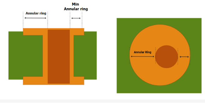
1. Understanding Annular Rings in PCB Design
1.1 Definition and Purpose
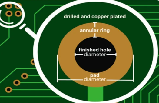
An annular ring refers to the copper pad area surrounding a drilled hole (via) on a PCB. It forms a conductive connection between the via barrel (plated hole) and the surrounding copper trace or plane. The primary functions of annular rings include:
- Electrical Connectivity: Ensures a reliable connection between the via and the conductive layers.
- Mechanical Stability: Provides structural support to prevent via breakout or detachment during fabrication and assembly.
- Thermal Management: Helps dissipate heat generated during soldering or operation.
1.2 Types of Vias and Their Annular Rings
Different via types require specific annular ring considerations:
- Through-Hole Vias: Span the entire PCB, requiring annular rings on all layers.
- Blind Vias: Connect an outer layer to an inner layer, with annular rings only on the connected layers.
- Buried Vias: Exist between inner layers, requiring annular rings only on the connected internal layers.
- Microvias: Smaller vias (typically <0.15mm) used in high-density designs, requiring precise annular ring control.
2. Importance of Proper Annular Ring Design
2.1 Preventing Via Breakout
A via breakout occurs when the drilled hole is misaligned, causing insufficient copper around the via. This can lead to:
- Open Circuits: If the annular ring is too thin, the via may lose electrical connectivity.
- Weak Mechanical Bonds: Poor annular rings increase the risk of via detachment during thermal cycling or mechanical stress.
2.2 Ensuring Signal Integrity
In high-frequency and high-speed PCBs, improper annular rings can cause:
- Impedance Discontinuities: Affecting signal propagation.
- Increased Crosstalk: Due to insufficient copper isolation.
2.3 Facilitating Manufacturing Yield
PCB fabrication involves drilling tolerances (±0.05mm to ±0.1mm). A sufficient annular ring compensates for drill misalignment, improving yield and reducing defects.
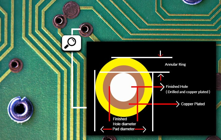
3. Design Considerations for Annular Rings
3.1 Minimum Annular Ring Requirements
Industry standards (IPC-2221, IPC-A-600) define minimum annular ring widths:
- Class 1 (General Electronics): ≥0.05mm (2 mils)
- Class 2 (Industrial/Telecom): ≥0.075mm (3 mils)
- Class 3 (High-Reliability/Aerospace): ≥0.1mm (4 mils)
3.2 Drill-to-Copper Clearance
The annular ring must account for:
- Drill Tolerance: Typically ±0.075mm.
- Copper Etching Variations: Over-etching can reduce annular ring width.
3.3 Pad Size Calculation
The pad diameter should be:
[
\text{Pad Diameter} = \text{Drill Diameter} + 2 \times \text{Annular Ring Width}
]
For example, a 0.3mm drill with a 0.1mm annular ring requires a 0.5mm pad.
3.4 High-Density Designs (HDI PCBs)
In HDI PCBs, laser-drilled microvias require tighter annular rings (≥0.025mm). Techniques like via-in-pad and filled vias help maintain reliability.
4. Manufacturing Challenges and Solutions
4.1 Drill Misalignment
Problem: Drilling inaccuracies can reduce annular ring width.
Solution:
- Use optical alignment systems for precision.
- Increase annular ring width in critical areas.
4.2 Copper Thickness Variations
Problem: Uneven copper plating affects annular ring integrity.
Solution:
- Follow controlled impedance plating processes.
- Use tented vias (covered with solder mask) for protection.
4.3 Thermal Stress
Problem: Repeated thermal cycling (e.g., in reflow soldering) can crack annular rings.
Solution:
- Use filled and capped vias for better thermal resistance.
- Apply reinforced pad designs (e.g., teardrop-shaped pads).
5. Best Practices for Annular Ring Management
5.1 Follow IPC Standards
Adhere to IPC-2221 and IPC-7351 guidelines for annular ring sizing based on PCB class.
5.2 Use DFM (Design for Manufacturing) Checks
- Verify annular rings in DFM software (e.g., Valor, CAM350).
- Consult PCB manufacturers for their process capabilities.
5.3 Optimize for High-Speed Designs
- Ensure consistent annular rings in differential pairs to maintain impedance.
- Avoid non-functional pads in high-speed signal layers.
5.4 Implement Advanced Via Structures
- Via-in-Pad: Places vias directly under component pads (requires plating/filling).
- Buried/Blind Vias: Reduces annular ring complexity in multilayer PCBs.
6. Future Trends in Via and Annular Ring Technology
6.1 Smaller Annular Rings with Laser Drilling
Advancements in UV and CO₂ laser drilling enable microvias with ultra-thin annular rings (<0.02mm).
6.2 Additive Manufacturing (3D-Printed PCBs)
Emerging techniques allow direct metal printing, eliminating traditional annular ring constraints.
6.3 AI-Driven PCB Design Optimization
Machine learning tools can automatically adjust annular rings based on thermal and electrical simulations.
Conclusion
Annular rings are a fundamental aspect of via management in PCB design, impacting electrical performance, manufacturability, and reliability. By adhering to industry standards, optimizing design rules, and leveraging advanced fabrication techniques, engineers can ensure robust via structures that meet the demands of modern electronics. As PCB technology evolves toward higher densities and faster signal speeds, annular ring optimization will remain a critical factor in successful PCB development.
By implementing the best practices discussed in this article, designers can minimize defects, enhance signal integrity, and improve the overall quality of their PCB layouts.