
Assembly Outline in PCB Design: A Comprehensive Guide
Introduction
Printed Circuit Board (PCB) design is a complex process that involves multiple stages, from schematic capture to final assembly. One critical aspect of PCB design is the assembly outline, which defines the physical boundaries and mechanical constraints of the board during the manufacturing and assembly process. This article explores the importance of the assembly outline in PCB design, its key components, best practices for defining it, and common challenges faced during implementation.
1. What is an Assembly Outline in PCB Design?
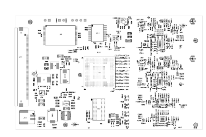
The assembly outline (also known as the board outline or fabrication outline) is a mechanical drawing layer in a PCB design that specifies the physical dimensions, shape, and critical features of the PCB. It serves as a reference for:
- PCB Fabrication: Determines how the board is cut (routed, scored, or V-cut).
- Component Placement: Guides where components can be placed without interfering with mechanical enclosures.
- Assembly Process: Ensures proper alignment during automated pick-and-place assembly.
- Testing & Inspection: Defines boundaries for test fixtures and optical inspection.
The assembly outline is typically defined in the CAD software (e.g., Altium Designer, KiCad, OrCAD) as a dedicated layer, often named “Mechanical Layer” or “Board Outline.”
2. Key Components of an Assembly Outline
A well-defined assembly outline includes the following elements:
2.1 Board Shape and Dimensions
- The exact length, width, and curvature of the PCB.
- Cutouts and slots for mounting or connectors.
- Internal cutouts (if the PCB has non-rectangular shapes).
2.2 Mounting Holes
- Specifies hole positions, diameters, and tolerances for screws or standoffs.
- Ensures compatibility with enclosures or mechanical fixtures.
2.3 Keepout Zones
- Areas where no components or traces should be placed (e.g., near edges or mounting points).
- Prevents interference with mechanical parts.
2.4 Fiducial Marks
- Optical alignment markers used in automated assembly to ensure accurate component placement.
- Typically placed near corners or critical components.
2.5 Tooling Holes
- Used for PCB alignment during fabrication and assembly.
- Ensures consistency in mass production.
2.6 Panelization Information (if applicable)
- Defines how multiple PCBs are arranged in a manufacturing panel.
- Includes breakaway tabs, V-grooves, or mouse bites for depanelization.
3. Best Practices for Defining an Assembly Outline
To ensure manufacturability and assembly efficiency, follow these best practices:
3.1 Use a Dedicated Layer in CAD Software
- Keep the assembly outline on a separate mechanical layer to avoid confusion with electrical layers.
- Clearly label it (e.g., “Board Outline” or “Mechanical 1”).
3.2 Maintain Proper Clearances
- Ensure minimum clearance between components and the board edge (typically 0.5mm–1mm).
- Avoid placing tall components near edges where they might interfere with enclosures.
3.3 Include Fiducials for Automated Assembly
- Place at least three fiducial marks (preferably global fiducials) for SMT assembly.
- Use non-solder-mask-covered copper pads for better machine recognition.
3.4 Define Keepout Zones for Critical Areas
- Mark areas where no copper, vias, or components should be placed (e.g., near mounting holes).
- Consider thermal and mechanical stress zones.
3.5 Verify with Mechanical Enclosures
- Cross-check the PCB outline with the mechanical CAD (MCAD) design to ensure fit.
- Account for tolerances in case of slight misalignments.
3.6 Follow Manufacturer’s Design Rules
- Consult the PCB fabrication house for minimum bend radius, slot widths, and hole tolerances.
- Avoid sharp internal corners (use fillets to reduce stress).
4. Common Challenges and Solutions
4.1 Incorrect Board Outline Leading to Fit Issues
- Problem: PCB doesn’t fit into the enclosure due to incorrect dimensions.
- Solution: Always verify with a 3D model and perform a DFM (Design for Manufacturability) check.
4.2 Missing Fiducials Causing Assembly Errors
- Problem: Pick-and-place machines misalign components.
- Solution: Always include fiducials and follow IPC-7351 standards.
4.3 Poorly Defined Keepout Zones
- Problem: Components placed too close to edges, causing assembly failures.
- Solution: Use automated DRC (Design Rule Check) to enforce keepout rules.
4.4 Panelization Mistakes Leading to Broken Boards
- Problem: PCBs break improperly during depanelization.
- Solution: Use proper tab spacing and V-scoring techniques.
5. Conclusion
The assembly outline is a crucial element in PCB design, bridging the gap between electrical and mechanical requirements. A well-defined outline ensures manufacturability, assembly accuracy, and reliability. By following best practices—such as maintaining clearances, adding fiducials, and verifying with mechanical designs—engineers can avoid costly errors and streamline production.
As PCBs become more complex with high-density interconnects (HDI) and flexible circuits, the importance of a precise assembly outline will only grow. By mastering this aspect, designers can enhance both the performance and manufacturability of their PCBs.