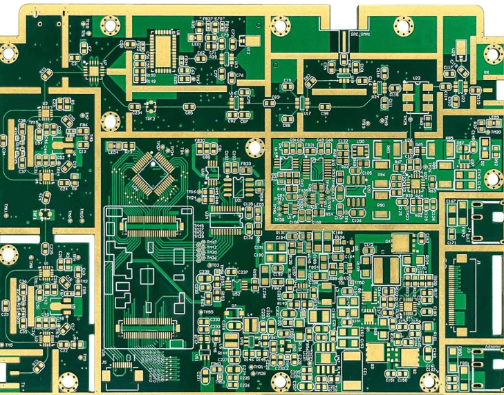
The shape and size design standards of pads in PCB design
I. Types of pads In general, pads can be divided into 7 categories, which are distinguished by shape as follows 2.Requirements for pads in PCB manufacturing process

I. Types of pads In general, pads can be divided into 7 categories, which are distinguished by shape as follows 2.Requirements for pads in PCB manufacturing process

1.The design of a printed circuit board starts with determining the size of the board. The size of the printed circuit board is limited by the size of the chassis shell, so it is best to fit it into the shell. Secondly, the connection method between the printed circuit board and external components (mainly potentiometers,…

For surface mount boards, especially BGA and IC mounting, the via plugging requirements must be flat, with a convex and concave of plus or minus 1mil, and the via edge must not be red and tinned; the via hole must not have tin beads. In order to meet customer requirements, the via plugging process can…

In general, stacking design mainly follows two rules: 1.Each routing layer must have an adjacent reference layer (power or ground layer); 2. The adjacent main power layer and ground layer must maintain a minimum spacing to provide a larger coupling capacitor; The following lists the stacking from two-layer boards to ten-layer boards: 3.Stacking of single-sided…

The security level of MCU is gradually improving, and some companies have even launched secure master controls. This is a good phenomenon, indicating that people are paying more and more attention to information security and program security in the embedded field. However, for many special industries, such as consumer electronics, low-cost communication modules, power control…

In the past two years, the word that everyone has heard the most is probably serial transmission. From the perspective of technological development, serial transmission has the momentum to completely replace parallel transmission. USB replaces IEEE 1284, SATA replaces PATA, and PCI Express replaces PCI. In principle, parallel transmission is actually better than serial transmission….

In addition to supporting various components in PCB boards, copper clad laminates can also achieve electrical connections or electrical insulation between them. 1.Classification of copper clad laminates Copper clad laminates are composed of three parts: copper foil, reinforcement material, and adhesive. Boards are usually classified according to the type of reinforcement material and adhesive type…

Generally, there are several reasons for copper cladding. 1.EMC. For large-area ground or power copper cladding It will play a shielding role. Some special grounds, such as PGND, play a protective role. 2.PCB process requirements. Generally, in order to ensure the electroplating effect or lamination deformation, copper is laid on PCB layers with less wiring….

1 Surface tension The cohesive force of tin-lead solder is even greater than that of water, making the solder spherical to minimize its surface area (under the same volume, the sphere has the smallest surface area compared to other geometric shapes to meet the requirements of the lowest energy state). The effect of flux is…

1 Line Generally, the signal line width is 0.3mm (12mil), and the power line width is 0.77mm (30mil) or 1.27mm (50mil); the distance between lines and between lines and pads is greater than or equal to 0.33mm (13mil). In practical applications, the distance should be increased when conditions permit;When the wiring density is high, it…

In any switching power supply design, the physical design of the PCB board is the last link. If the design method is not appropriate, the PCB may radiate too much electromagnetic interference, causing the power supply to work unstably. The following is an analysis of the matters that need to be paid attention to in…

Most of today’s mass-produced electronic hardware is manufactured using surface mount technology, or SMT. In addition to offering many other advantages, SMT PCBs go a long way in speeding up PCB production time. As we all know, Jieduobang’s expedited service and board delivery period are very fast, so we have a very big advantage in…

Via is one of the important components of multi-layer PCB, and the cost of drilling usually accounts for 30% to 40% of the cost of PCB board manufacturing. Simply put, every hole on the PCB can be called a via. From the perspective of function, vias can be divided into two categories: one is used…

With NB-IoT reaching 50 million shipments this year and expected to reach 100 million next year, it has risen rapidly. A medium-speed (including 3G, Cat.1, eMTC (catm)) market between high-speed (5G and 4G LTE) and low-speed (2G GPRS and NB-IoT) is emerging. The time for LTE Cat 1 to take on the main role of…

1.What is Immersion Gold? Simply put, Immersion Gold is a method of chemical deposition that produces a metal coating on the surface of the circuit board through a chemical oxidation-reduction reaction. 2.Why do we need Immersion Gold? The copper on the circuit board is mainly red copper. The copper solder joints are easily oxidized in…