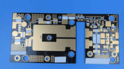
Author: Grace

  • Rf pcb prototyping

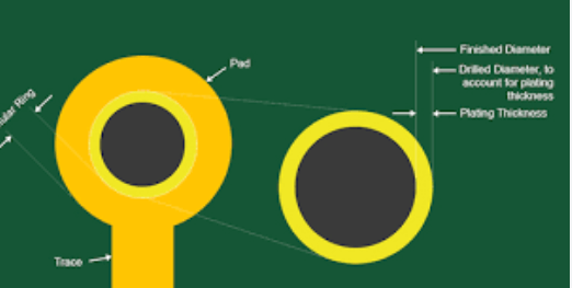
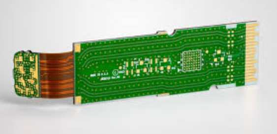
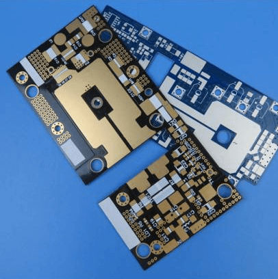
    Essential Design Tips For RF PCB Prototyping RF PCB prototyping is a critical phase in the development of radio frequency (RF) circuits, where precision and attention to detail are paramount. To ensure the success of your RF PCB prototype, it is essential to adhere to several design tips that can significantly impact performance and reliability….

  • Rf pcb routing guidelines

    Best Practices For RF PCB Routing When designing RF (Radio Frequency) printed circuit boards (PCBs), adhering to best practices for routing is crucial to ensure optimal performance and signal integrity. The complexity of RF signals, which operate at high frequencies, necessitates meticulous attention to detail in the PCB layout process. To begin with, one of…

  • Rf pcb rules

    Key Design Considerations for RF PCB Layout When designing a Radio Frequency (RF) Printed Circuit Board (PCB), several key considerations must be taken into account to ensure optimal performance and reliability. The complexity of RF signals, which operate at high frequencies, necessitates meticulous attention to detail in the layout process. One of the primary considerations…

  • Rf pcb shield

    Benefits Of Using RF PCB Shields In Modern Electronics In the realm of modern electronics, the utilization of RF PCB shields has become increasingly prevalent, driven by the need to enhance device performance and ensure electromagnetic compatibility. RF PCB shields, or Radio Frequency Printed Circuit Board shields, serve as protective barriers that mitigate the adverse…

  • Rf pcb simulation

    Introduction To RF PCB Simulation: Key Concepts And Tools RF PCB simulation is a critical process in the design and development of radio frequency printed circuit boards. This simulation involves the use of specialized software tools to model and analyze the behavior of RF circuits before they are physically manufactured. By simulating the performance of…

  • Rf pcb solder mask

    Importance Of Solder Mask In Rf pcb solder mask In the realm of Radio Frequency (RF) Printed Circuit Board (PCB) design, the solder mask plays a pivotal role in ensuring the functionality and reliability of the final product. The solder mask, a thin layer of polymer applied to the copper traces of a PCB, serves…

  • Rf pcb substrates

    Understanding The Basics Of RF PCB Substrates In the realm of modern electronics, the importance of Radio Frequency (RF) Printed Circuit Boards (PCBs) cannot be overstated. These specialized PCBs are integral to the functionality of a wide array of devices, from smartphones to sophisticated communication systems. Central to the performance of RF PCBs are the…

  • Rf pcb surface finish

    Advantages Of Rf pcb surface finish Electroless Nickel Immersion Gold (ENIG) surface finish has become a popular choice for Radio Frequency (RF) Printed Circuit Boards (PCBs) due to its numerous advantages. One of the primary benefits of using ENIG surface finish for RF PCBs is its excellent electrical performance. The combination of nickel and gold…

  • Rf pcb test probe

    Understanding The Basics Of RF PCB Test Probes RF PCB test probes are essential tools in the realm of electronics, particularly in the testing and validation of radio frequency (RF) printed circuit boards (PCBs). These probes are designed to facilitate the accurate measurement and analysis of high-frequency signals, ensuring that the PCBs function correctly within…

  • Rf pcb trace

    Designing Efficient RF PCB Traces for High-Frequency Applications Designing efficient RF PCB traces for high-frequency applications is a critical aspect of modern electronics engineering. As the demand for faster and more reliable wireless communication systems continues to grow, the need for precise and effective RF PCB trace design becomes increasingly important. This process involves a…

  • Rf pcb transmission line

    Design Techniques For RF PCB Transmission Lines Designing RF PCB transmission lines requires a meticulous approach to ensure signal integrity and minimize losses. The first step in this process involves selecting the appropriate substrate material, as the dielectric constant and loss tangent of the substrate significantly impact the performance of the transmission line. Common materials…

  • Rf pcb via diameter

    Importance Of Via Diameter In RF PCB Design In the realm of Radio Frequency (RF) Printed Circuit Board (PCB) design, the importance of via diameter cannot be overstated. Vias, which are small conductive pathways that connect different layers of a PCB, play a crucial role in ensuring signal integrity and overall performance. The diameter of…

  • Rf pool pcb

    Designing Efficient RF Pool PCB Layouts Designing efficient RF pool PCB layouts is a critical task that demands meticulous attention to detail and a deep understanding of both electrical and mechanical principles. The primary objective is to ensure optimal performance while minimizing interference and signal loss. To achieve this, several key factors must be considered…

  • Rf power amplifier pcb layout

    Key Design Considerations for RF Power Amplifier PCB Layout When designing a printed circuit board (PCB) for an RF power amplifier, several key considerations must be taken into account to ensure optimal performance and reliability. The layout of the PCB plays a crucial role in determining the efficiency, signal integrity, and thermal management of the…

  • Rf shield box pcb

    Design Considerations for RF Shield Box PCB When designing a printed circuit board (PCB) for an RF shield box, several critical considerations must be taken into account to ensure optimal performance and functionality. The primary objective of an RF shield box is to isolate sensitive electronic components from external electromagnetic interference (EMI) and to prevent…