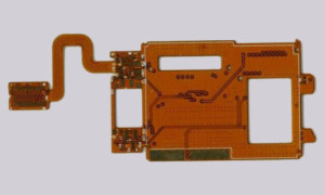
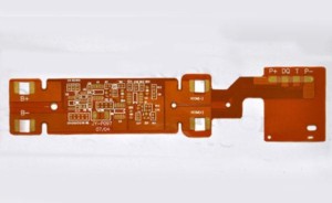
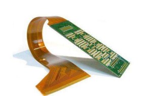
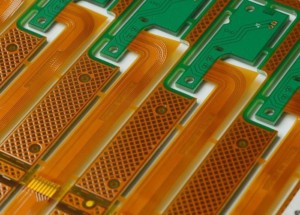
Author: Grace

  • |

    High speed pcb design with emi resilience

    High-speed PCB design with EMI resilience is a critical aspect of electronic product development. 1. Grounding and shielding: Proper grounding and shielding techniques can help reduce EMI emissions and improve immunity.Use a solid ground plane and separate analog and digital grounds. Shield sensitive components and traces. 2. Signal routing: Keep high-speed signal traces as short…

  • |

    High speed interfaces in pcb

    High speed interfaces in PCB (Printed Circuit Board) refer to the communication links between electronic components that operate at high frequencies, typically in the range of several hundred MHz to several GHz. These interfaces are used in various applications such as data communication, video transmission, and high-speed computing. Some of the common high-speed interfaces used…

  • |

    What is high speed pcb design

    High speed PCB design refers to the process of designing printed circuit boards that can handle high frequency signals without signal degradation or loss.This is achieved by carefully selecting components, using proper trace routing techniques,and minimizing electromagnetic interference (EMI) and crosstalk. High speed PCB design is essential for electronic devices that require fast data transfer…

  • |

    High speed pcb materials

    High speed PCB materials are materials that are used to manufacture high-speed printed circuit boards (PCBs) that can handle high-frequency signals and provide reliable performance. These materials have low dielectric constant (Dk) and low dissipation factor (Df), which reduces signal loss and distortion. 1. FR-4: This is a popular material for high-speed PCBs due to…

  • |

    High speed pcb design guidelines

    1. High-Speed Digital Design: A Handbook of Black Magic by Howard Johnson and Martin Graham2. Signal and Power Integrity – Simplified by Eric Bogatin3. Principles of Signal Integrity by Dr. Howard Johnson4. PCB Design for High-Speed Digital Systems by Dr. Lee Ritchey5. High-Speed PCB Design Considerations by Altium6. High-Speed Board Design Techniques by Cadence7. High-Speed…

  • |

    High speed pcb

    High speed PCB manufacturing What is High speed PCB? High-speed PCB is a kind of PCB board manufactured with high-speed PCB material,which has the characteristics of high speed, high reliability, low delay,large capacity, and high bandwidth. In the 1990s digital signaling in electronics in 100 Mhz range was “high speed”. Chips and computer performance have…

  • |

    Thermal pad pcbox

    PCBox is a company that specializes in the distribution of electronic components and products.They offer a wide range of thermal pads that are designed to provide thermal management solutions for various electronic applications. These thermal pads are made of high-quality materials such as silicone, graphite, and ceramic,and are available in different sizes, thicknesses, and thermal…

  • |

    Pcb thermal pad calculator

    There are several online calculators available to help determine the appropriate size of a thermal pad for a specific component.Here are a few popular options: 1. PCB Thermal Calculator by Saturn PCB Design: This calculator allows you to input the component package type, power dissipation,and PCB copper thickness to determine the recommended thermal pad size….

  • |

    Pcb thermal pad vias

    PCB thermal pad vias are typically used in electronic devices that generate a lot of heat,such as microprocessors, power amplifiers, and voltage regulators. The thermal pad via is used to transfer heat from the component to the ground plane of the PCB,which helps to dissipate the heat and prevent damage to the component. The thermal…

  • |

    How thermal pad works

    A thermal pad works by providing a thermal interface between two surfaces,typically a heat-generating component and a heat sink or PCB. The thermal pad is made of a soft, thermally conductive material that fills any gaps or imperfections between the two surfaces,allowing heat to transfer more efficiently. When a component generates heat, it needs to…

  • |

    Thermal pad pcb layout

    There should be sufficient clearance around the thermal pad to avoid short circuits and ensure proper soldering. 4. Solder mask: The solder mask should be removed from the thermal pad to allow for proper soldering. 5. Via placement: Vias can be placed around the thermal pad to improve heat dissipation and reduce thermal resistance. 6….

  • |

    what is a thermal pad

    A thermal pad is a type of thermal interface material (TIM) that is used to transfer heat between two surfaces.It is typically made of a soft, compressible material such as silicone or graphite that is infused with thermally conductive particles. When placed between a heat-generating component, such as a CPU or GPU, and a heat…