Automated Optical Inspection (AOI): Revolutionizing Quality Control in Manufacturing
Introduction to AOI Technology
Automated Optical Inspection (AOI) has emerged as a transformative force in modern manufacturing quality control, particularly in electronics production. This advanced technology utilizes high-resolution cameras, sophisticated lighting systems, and complex image processing algorithms to automatically detect defects and verify quality in manufactured products with unprecedented speed and accuracy.
AOI systems represent a significant leap forward from traditional manual inspection methods, offering manufacturers the ability to maintain rigorous quality standards while meeting the demands of high-volume production. As components continue to shrink in size and circuit boards grow in complexity, AOI has become not just advantageous but essential for maintaining product reliability and manufacturing efficiency.
The Core Components of AOI Systems
A typical AOI system consists of several key components that work in harmony to deliver precise inspection results:
Imaging System: At the heart of every AOI machine are high-resolution cameras, often combining multiple sensors with different resolutions and capabilities. Modern systems may use area scan cameras, line scan cameras, or specialized 3D imaging technology depending on the application requirements. These cameras capture detailed images of the product under inspection with pixel resolutions that can detect sub-micron level defects.
Lighting Technology: Advanced illumination systems are crucial for highlighting potential defects. AOI systems employ various lighting techniques including:
- Coaxial lighting for reflective surfaces
- Dark field illumination for surface irregularities
- Structured light for 3D measurements
- Multi-spectral lighting for different material properties
Motion Control System: Precision mechanics ensure accurate positioning of either the camera system or the product being inspected. High-precision linear motors, servo systems, and vibration-dampening structures maintain stability during high-speed operations.
Computing Platform: Powerful processors running specialized software perform real-time image analysis. Modern systems incorporate GPU acceleration and sometimes even AI coprocessors to handle the enormous computational demands of high-speed, high-resolution inspection.
Software Algorithms: The “intelligence” of AOI systems resides in their software, which typically includes:
- Pattern matching algorithms
- Statistical pattern recognition
- Neural networks and deep learning models
- Defect classification systems
- Measurement and verification tools
AOI Applications Across Industries
While initially developed for printed circuit board (PCB) inspection, AOI technology has found applications across numerous manufacturing sectors:
Electronics Manufacturing:
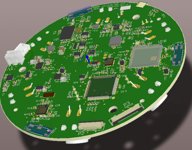
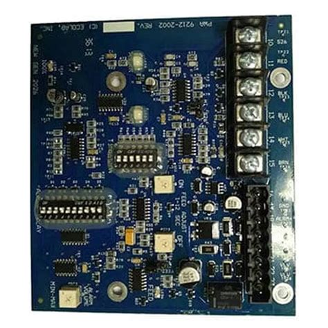
- PCB assembly verification (solder joints, component placement)
- Semiconductor wafer inspection
- Display panel inspection (LCD, OLED)
- Connector and cable assembly verification
Automotive Industry:
- Inspection of electronic control units
- Lighting component verification
- Safety-critical component inspection
- Surface finish quality control
Medical Device Manufacturing:
- Micro-component inspection
- Surgical instrument verification
- Implant device quality control
- Packaging integrity checks
General Manufacturing:
- Dimensional measurement of precision parts
- Surface defect detection
- Label and marking verification
- Assembly completeness checks
Advantages of AOI Implementation
The adoption of AOI technology offers manufacturers numerous competitive advantages:
Enhanced Quality Control: AOI systems can detect defects that are imperceptible to human inspectors, including microscopic cracks, slight discoloration, or minute dimensional variations. The consistency of automated inspection eliminates human fatigue factors and maintains constant vigilance throughout production runs.
Increased Throughput: Modern AOI systems can inspect hundreds or even thousands of components per minute, far surpassing manual inspection capabilities. This high-speed operation enables 100% inspection rather than statistical sampling in many applications.
Cost Reduction: By catching defects early in the production process, AOI reduces scrap and rework costs. The technology also minimizes the need for large quality control staffs and reduces liability from field failures.
Data-Driven Process Improvement: AOI systems generate vast amounts of inspection data that can be analyzed to identify process trends, predict equipment maintenance needs, and continuously improve manufacturing processes.
Flexibility and Adaptability: Modern AOI systems can be quickly reprogrammed for new products, allowing manufacturers to respond rapidly to design changes or new product introductions.
Technical Challenges in AOI Implementation
Despite its advantages, AOI implementation presents several technical challenges that must be addressed:
False Call Rates: Balancing sensitivity to avoid both false negatives (missed defects) and false positives (good parts flagged as defective) requires careful system tuning. Advanced algorithms and machine learning techniques are increasingly used to optimize this balance.
Complex Component Geometries: As components become more three-dimensional with finer pitches and hidden connections, inspection systems must evolve with more sophisticated imaging techniques and viewing angles.
Surface Variability: Shiny, reflective, or textured surfaces can challenge traditional imaging systems, requiring advanced lighting solutions and algorithmic approaches.
High-Mix Production: Facilities producing many different products in small batches need AOI systems that can quickly adapt to new inspection requirements without extensive reprogramming.
Data Management: The large volume of image data generated by high-speed AOI systems requires robust data storage, processing, and analysis infrastructure.
Emerging Trends in AOI Technology
The field of automated optical inspection continues to evolve with several notable trends:
AI and Deep Learning Integration: Modern AOI systems increasingly incorporate artificial intelligence, particularly deep learning neural networks, to improve defect recognition and classification. These systems can learn from examples rather than relying solely on programmed rules, enabling better handling of complex or variable defects.
3D Inspection Capabilities: Advanced systems now combine multiple imaging angles or structured light projection to create three-dimensional models of inspected components, allowing for more comprehensive verification of height-related features like solder joint quality.
In-Line Process Control: Rather than simply detecting defects at the end of the line, AOI systems are being integrated into production processes to provide real-time feedback for process adjustment, preventing defect generation rather than just detecting bad product.
Multi-Spectral Imaging: Systems incorporating infrared, ultraviolet, or hyperspectral imaging capabilities can detect defects or material properties not visible in standard visible light inspection.
Edge Computing Architecture: Distributing some of the image processing to edge devices near the inspection point reduces latency and network bandwidth requirements while enabling faster response times.
Augmented Reality Interfaces: New human-machine interfaces for AOI systems use AR to help operators quickly understand defects and system status, reducing training time and improving responsiveness.
The Future of AOI Technology
Looking ahead, several developments promise to further enhance AOI capabilities:
Quantum Imaging Sensors: Emerging sensor technologies may provide unprecedented sensitivity and speed for defect detection.
Predictive Quality Analytics: Combining AOI data with other process data using advanced analytics will enable predictive quality control, anticipating defects before they occur.
Self-Learning Systems: AOI systems that continuously improve their inspection capabilities based on new data without explicit reprogramming.
Nanoscale Inspection: As components approach atomic scales, AOI systems will need to integrate with electron microscopy and other nanoscale imaging techniques.
Closed-Loop Manufacturing Systems: Tight integration of AOI with production equipment will create fully adaptive manufacturing systems that automatically adjust processes to maintain optimal quality.
Conclusion
Automated Optical Inspection has become an indispensable tool in modern manufacturing, particularly in electronics where miniaturization and complexity have made manual inspection impractical. As the technology continues to evolve with AI integration, advanced imaging techniques, and smarter data analytics, AOI systems will play an even greater role in ensuring product quality while enabling faster, more efficient manufacturing processes.
The future of AOI lies not just in better defect detection, but in the complete integration of inspection data into the manufacturing ecosystem, creating intelligent, self-optimizing production lines that can maintain quality standards autonomously. For manufacturers looking to compete in an increasingly demanding global market, investment in advanced AOI technology is not just an option—it’s a necessity for survival and growth.