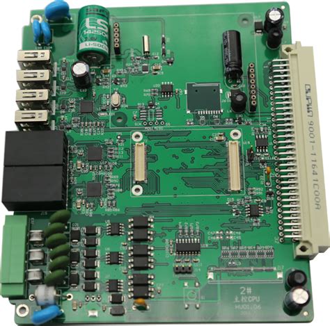
(COB) Chip on Board (COB) packaging welding method and packaging process
The chip on board (COB) process first covers the silicon wafer placement point on the substrate surface with thermal conductive…
Blogs
The chip on board (COB) process first covers the silicon wafer placement point on the substrate surface with thermal conductive…
In a single in-line package (SIP), the pins are led out from one side of the package and arranged in…
Dry film solder mask is not in liquid or paste form, it appears in the form of a photosensitive polymer…
Most of the design performance of multi-substrates is similar to that of single or dual substrates, that is, to avoid…
The ability to control machines with thoughts is a long-standing dream; especially for those who are paralyzed. In recent years,…
The situation involving moisture sensitivity of plastic integrated circuits (ICs) has been steadily getting worse, due to a number of…

I. Circuit online test technology In order to ensure the functional test of the device on the circuit board, the…
Protective coating is used to enhance the performance and reliability of printed circuit board assemblies, enabling them to be used…

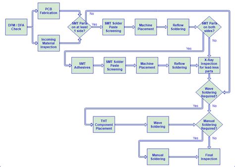
This article explores cutting-edge strategies in PCB production and assembly processes, highlighting advancements in technology, efficiency improvements, and best practices to optimize quality and reduce costs in the electronics industry.
Explore the process of getting custom PCBs made for your personalized keyboard projects. From design to manufacturing, learn how to create unique layouts that suit your needs, including options for low-profile switches and split designs.
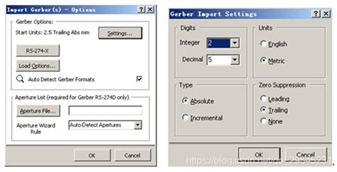
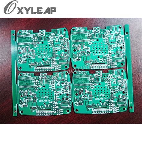
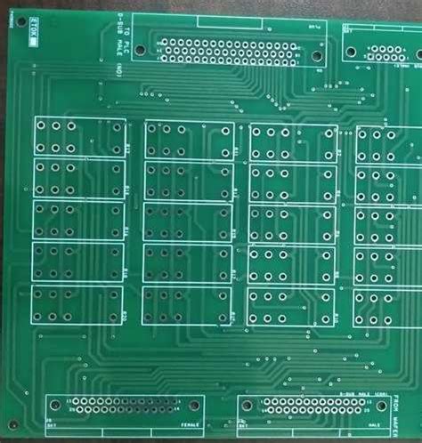
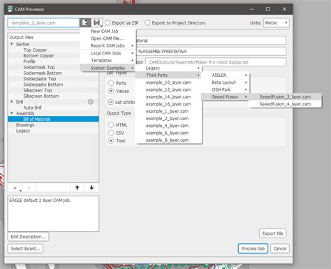
This article guides you through the process of transforming Gerber files into functional PCB layouts. Learn the essential steps to recreate your designs efficiently and effectively while minimizing the challenges of manual layout redos.
Discover essential techniques for PCB circuit board assembly that enhance efficiency and ensure top-notch quality. This article provides valuable insights and best practices to streamline your assembly process and achieve optimal results.
Discover how to enhance your quick PCB assembly workflow with efficient strategies and best practices. Learn to streamline processes, reduce turnaround times, and improve overall productivity for faster results in your projects.
This article explores the importance of Gerber files in the PCB design process, detailing how they facilitate manufacturing by providing crucial layout information for custom PCB production. Ideal for both novices and experienced designers.
In the design of electronic systems, in order to avoid detours and save time, the requirements for anti-interference should be…
We use cookies to improve your experience on our site. By using our site, you consent to cookies.
Manage your cookie preferences below:
Essential cookies enable basic functions and are necessary for the proper function of the website.
Statistics cookies collect information anonymously. This information helps us understand how visitors use our website.
Google Analytics is a powerful tool that tracks and analyzes website traffic for informed marketing decisions.
Service URL: policies.google.com (opens in a new window)
SourceBuster is used by WooCommerce for order attribution based on user source.
You can find more information in our privacy policy and privacy policy.