Ceramic PCB Material Selection Guide: Matching Substrate to Your Application Requirements
Selecting the right ceramic substrate for your PCB project directly impacts thermal performance, electrical reliability, and long-term cost efficiency. This guide breaks down the technical parameters that matter most when choosing between alumina (Al2O3), aluminum nitride (AlN), and beryllium oxide (BeO) substrates for high-power, high-frequency, and thermally demanding applications.
Table of Contents
- Why Ceramic PCB Material Selection Matters for Your Design
- Key Material Properties Explained: Thermal Conductivity, Dielectric Constant, and CTE
- Ceramic Substrate Comparison: Al2O3 vs AlN vs BeO
- Application-Driven Material Selection Framework
- Design Considerations for Ceramic PCB Manufacturability
- Cost vs Performance Trade-offs in Ceramic PCB Selection
- FAQ
- Conclusion and Next Steps
1. Why Ceramic PCB Material Selection Matters for Your Design
Ceramic PCB substrates serve applications where standard FR4 fails under thermal stress, high-frequency signal degradation, or dimensional stability requirements. Power electronics modules operating above 150°C, RF amplifiers in the 5G infrastructure, and automotive LED drivers all require substrates that combine high thermal conductivity with electrical insulation.
The wrong substrate choice shows up as premature device failure, signal integrity issues at higher frequencies, or excessive thermal resistance leading to derating. For a 100W LED module, switching from standard alumina to aluminum nitride can reduce junction temperature by 15-20°C, directly extending LED lifespan by 30-40%. For RF power amplifiers, substrate dielectric constant (Dk) and loss tangent (Df) determine whether your design meets insertion loss and return loss specifications.
Material selection must account for three constraints simultaneously: thermal management requirements, electrical performance targets, and manufacturing cost limits. A high-power IGBT module may need AlN for its thermal conductivity, but if the application operates below 125°C and cost is constrained, alumina with enhanced thermal design may suffice. This guide provides the decision framework and technical data needed to match substrate properties to your specific application requirements.
2. Key Material Properties Explained: Thermal Conductivity, Dielectric Constant, and CTE
Thermal Conductivity (W/m·K)
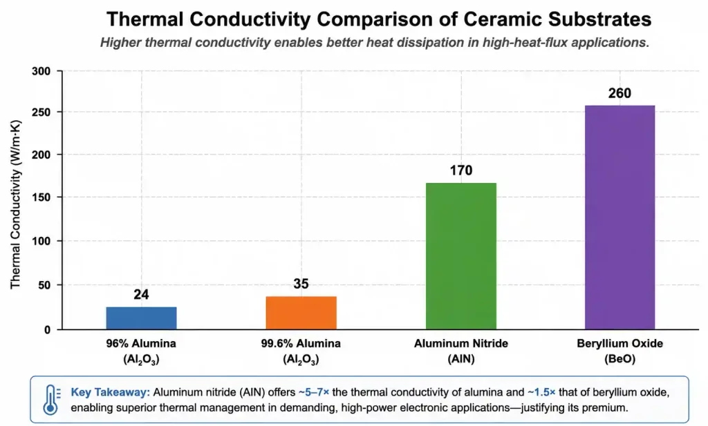
Thermal conductivity determines how effectively the substrate transfers heat from active devices to the heat sink or ambient environment. For power electronics, this property directly controls junction temperature and thermal resistance (Rth). A substrate with 170 W/m·K thermal conductivity (aluminum nitride) spreads heat three times faster than 96% alumina at 24 W/m·K.
In practice, thermal conductivity must be evaluated alongside substrate thickness. For a 0.635 mm thick substrate, each 50 W/m·K increase in thermal conductivity reduces thermal resistance by approximately 0.8 K/W per square centimeter. This becomes critical in applications where junction-to-case thermal resistance must stay below 1.0 K/W to prevent thermal runaway.
Dielectric Constant (Dk) and Loss Tangent (Df)
Dielectric constant affects impedance control and signal propagation speed in RF and high-speed digital designs. Alumina’s Dk of 9.8 at 1 MHz requires narrower trace widths for 50-ohm impedance compared to FR4. Aluminum nitride at Dk 8.9 offers slightly better performance, but the high Dk of all ceramic substrates means microstrip and stripline calculations must account for tighter coupling and reduced trace-to-ground clearances.
Loss tangent determines high-frequency signal attenuation. At 10 GHz, alumina’s Df of 0.0003 results in roughly 0.2 dB/inch insertion loss for a 50-ohm microstrip, making it suitable for frequencies up to 40 GHz. Beryllium oxide offers even lower loss tangent (0.0001), but handling restrictions limit its use to specialized military and aerospace applications.
Coefficient of Thermal Expansion (CTE)
CTE mismatch between substrate and copper metallization or between substrate and die attach creates thermomechanical stress during temperature cycling. Alumina’s CTE of 6.7 ppm/°C closely matches copper at 16.5 ppm/°C better than aluminum nitride at 4.5 ppm/°C. However, AlN’s CTE is nearly identical to silicon (3.5 ppm/°C) and gallium nitride (5.3 ppm/°C), making it preferable for direct die attach in power semiconductor modules.
For assemblies subjected to -40°C to 150°C automotive qualification cycling, CTE-driven solder fatigue becomes the dominant failure mode. Finite element analysis should verify that shear stress at the die-substrate interface stays below 50 MPa across the temperature range, which often requires matching substrate CTE to the semiconductor material rather than to the copper traces.
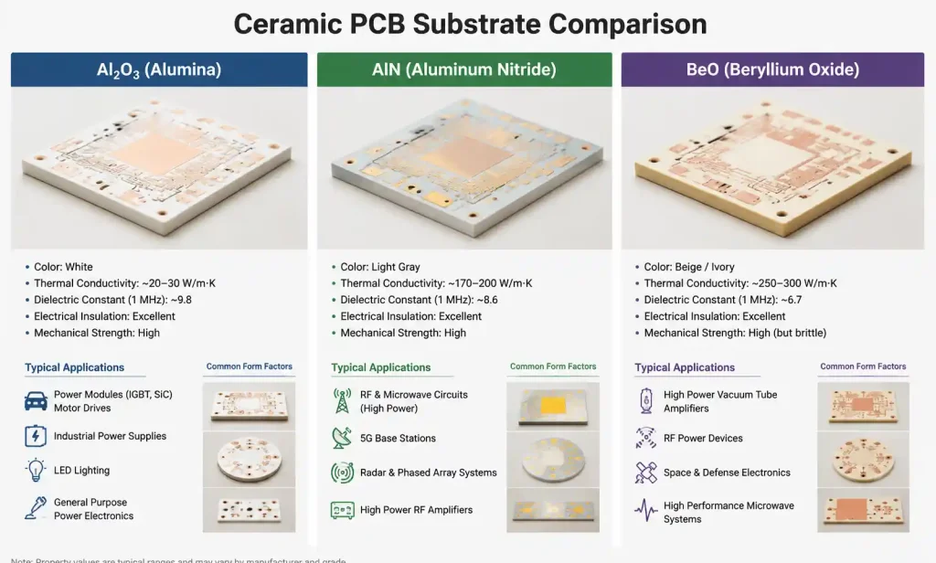
3. Ceramic Substrate Comparison: Al2O3 vs AlN vs BeO
| Property | 96% Alumina | 99.6% Alumina | Aluminum Nitride | Beryllium Oxide |
|---|---|---|---|---|
| Thermal Conductivity (W/m·K) | 24 | 35 | 170–180 | 250–280 |
| Dielectric Constant (1 MHz) | 9.8 | 9.9 | 8.9 | 6.7 |
| Loss Tangent (10 GHz) | 0.0003 | 0.0002 | 0.0010 | 0.0001 |
| Flexural Strength (MPa) | 350 | 450 | 320 | 250 |
| CTE (ppm/°C, 25–400°C) | 6.7 | 6.8 | 4.5 | 7.5 |
| Volume Resistivity (Ω·cm) | >10¹⁴ | >10¹⁴ | >10¹³ | >10¹⁴ |
| Max Operating Temp (°C) | 1600 | 1700 | 1200 | 2000 |
| Relative Cost (96% Al2O3 = 1.0) | 1.0 | 1.3 | 4.5–5.5 | 12–15 |
This comparison shows the fundamental trade-off between thermal performance and cost. Aluminum nitride’s thermal conductivity advantage justifies its 4.5× cost premium only when thermal resistance calculations show that alumina cannot meet junction temperature requirements. For designs where heat flux exceeds 50 W/cm², AlN becomes necessary to maintain semiconductor junction temperature within safe operating limits.
The higher loss tangent of AlN (0.0010 vs 0.0003 for alumina) matters primarily above 20 GHz. For typical power electronics switching frequencies (20 kHz to 500 kHz) and for RF applications below 10 GHz, both materials provide adequate dielectric performance. Beryllium oxide offers the best combination of thermal and electrical properties but requires specialized handling protocols due to beryllium toxicity, restricting its use to aerospace and defense applications where no alternative meets specifications.
Material purity affects both cost and performance. The jump from 96% to 99.6% alumina increases thermal conductivity by 45% but adds 30% to material cost. For high-volume automotive applications, 96% alumina often provides the best cost-performance balance, while telecommunications infrastructure and industrial motor drives justify 99.6% alumina or AlN for improved reliability.
4. Application-Driven Material Selection Framework
High-Power LED and Solid-State Lighting
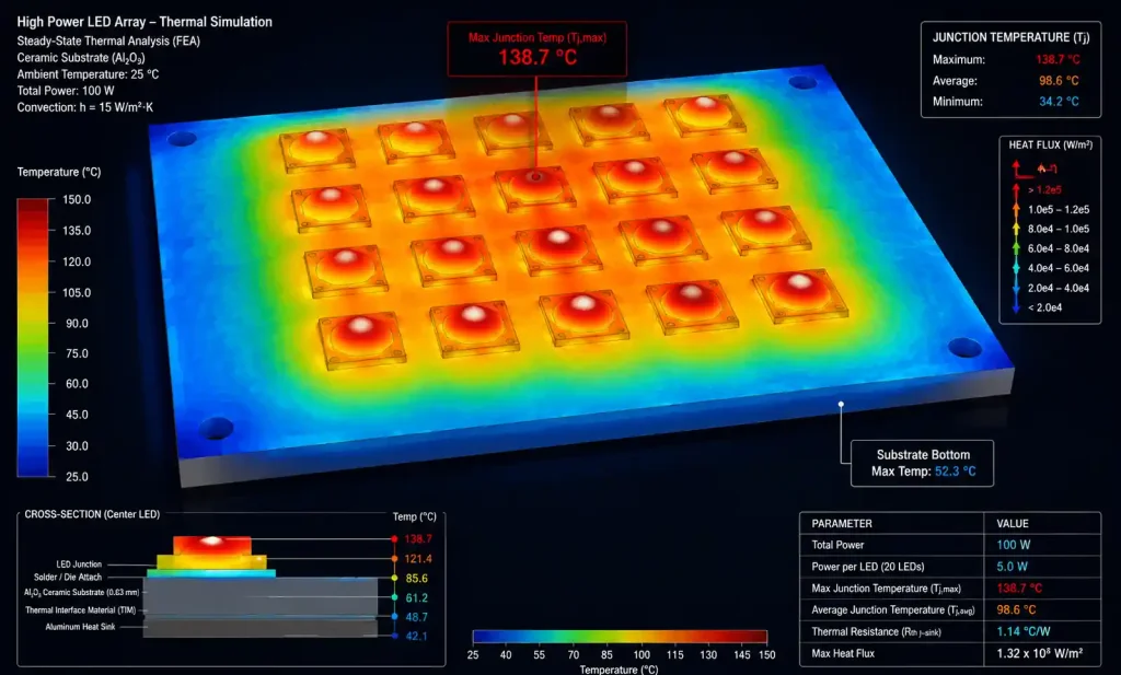
LED thermal management requires substrates that extract heat efficiently while maintaining electrical isolation between LED junctions. For mid-power LEDs (0.5–3W per package), 96% alumina suffices when combined with adequate heat sinking. High-power COB (chip-on-board) LED arrays above 50W total power require aluminum nitride to keep junction temperature below 120°C for L70 lifetimes exceeding 50,000 hours.
Design rule: calculate heat flux (W/cm²) at the LED die footprint. If heat flux exceeds 30 W/cm², aluminum nitride is necessary. Below 15 W/cm², alumina works well. Between 15–30 W/cm², compare thermal simulation results for both materials against your junction temperature target.
Power Electronics and IGBT Modules
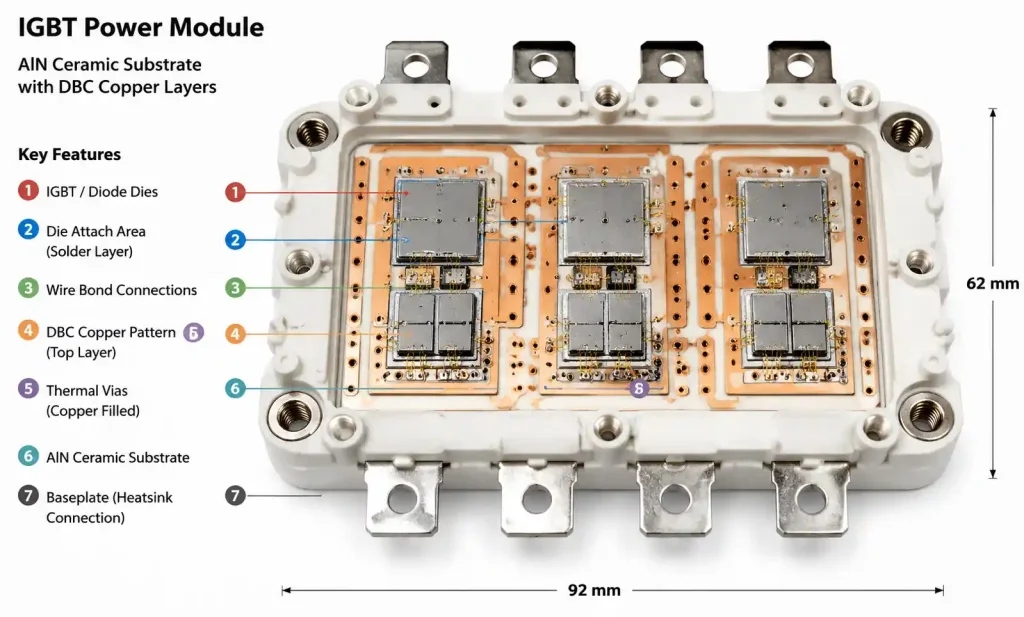
IGBT and MOSFET power modules for motor drives, solar inverters, and EV traction inverters generate concentrated heat during switching transients. Aluminum nitride’s high thermal conductivity allows direct bonded copper (DBC) substrates to handle 200–300 A current with acceptable junction-to-case thermal resistance. The CTE match to silicon (for silicon IGBTs) or silicon carbide (for SiC MOSFETs) also improves solder joint reliability under power cycling.
For automotive-qualified modules meeting AQG324 requirements (2000 thermal cycles, -40°C to 150°C), AlN substrates reduce thermomechanical stress at the die attach interface by 25–30% compared to alumina, directly translating to improved power cycling capability. This benefit justifies the substrate cost premium in EV applications where field failure rates must stay below 10 PPM.
RF and Microwave Amplifiers
RF power amplifiers for 5G base stations, radar systems, and satellite communications require substrates with low dielectric loss and stable electrical properties across temperature. For frequencies below 10 GHz, 99.6% alumina provides adequate performance with insertion loss below 0.3 dB/inch. Above 20 GHz, BeO’s lower loss tangent becomes necessary for multi-stage amplifier designs where cumulative insertion loss must stay below 1.0 dB.
Thermal management remains critical even in RF applications because RF power amplifiers operate at 40–50% efficiency, dissipating significant heat. GaN-on-SiC RF devices benefit from AlN substrates that provide both excellent thermal conductivity and CTE matching to the GaN die.
Automotive Electronics
Automotive underhood electronics (ECU, power distribution modules, LED drivers) must survive -40°C to 150°C ambient with 3000+ thermal cycles. Alumina substrates dominate this space due to proven reliability and cost effectiveness. The substrate must meet AEC-Q200 qualification and maintain dielectric strength above 15 kV/mm after temperature-humidity-bias (THB) testing.
For high-power applications like 800V EV inverters, aluminum nitride enables higher power density and improved efficiency through reduced thermal resistance. The cost premium is accepted because it allows smaller, lighter inverter designs that improve vehicle range and packaging.
| Application | Recommended Substrate | Key Selection Driver | Typical Thickness |
|---|---|---|---|
| Mid-power LED (< 3W) | 96% Al2O3 | Cost, adequate thermal performance | 0.635 mm |
| High-power LED (> 50W COB) | AlN | High heat flux, junction temp control | 0.635–1.0 mm |
| Silicon IGBT modules | AlN | Thermal performance, CTE matching | 0.635–1.0 mm |
| SiC MOSFET modules | AlN | Thermal + CTE matching to SiC | 0.380–0.635 mm |
| RF amplifier (< 10 GHz) | 99.6% Al2O3 | Dielectric loss, cost | 0.635–1.0 mm |
| RF amplifier (> 20 GHz) | BeO (or Al2O3) | Low loss tangent | 0.254–0.635 mm |
| Automotive ECU | 96% Al2O3 | Cost, reliability, AEC-Q200 | 0.635 mm |
| EV traction inverter | AlN | High power density, efficiency | 0.635–1.0 mm |
This table provides initial guidance, but final substrate selection must be validated through thermal simulation and stress analysis for your specific design. Heat flux, junction temperature limits, and power cycling requirements determine whether the lower-cost option meets reliability targets or whether premium materials are necessary.
5. Design Considerations for Ceramic PCB Manufacturability
Substrate Thickness and Copper Layer Configuration
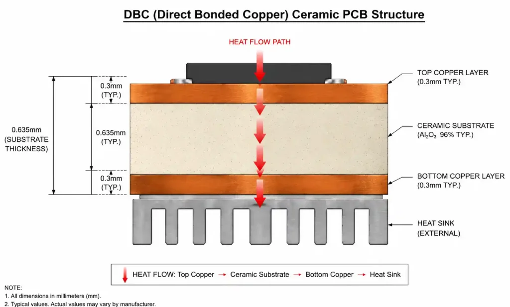
Ceramic PCB substrates are available in standard thicknesses: 0.254 mm, 0.380 mm, 0.635 mm, and 1.0 mm. Thinner substrates provide lower thermal resistance but reduced mechanical strength and higher fragility during handling. For power electronics, 0.635 mm represents the best balance between thermal performance and manufacturing yield.
Copper metallization uses direct bonded copper (DBC) or active metal brazing (AMB) processes. DBC typically provides 0.2–0.6 mm copper thickness, with 0.3 mm being most common for power electronics. Thicker copper (0.4–0.6 mm) handles higher current but increases manufacturing cost and minimum feature size. AMB allows thinner copper layers (0.1–0.2 mm) with finer trace widths, suitable for RF designs.
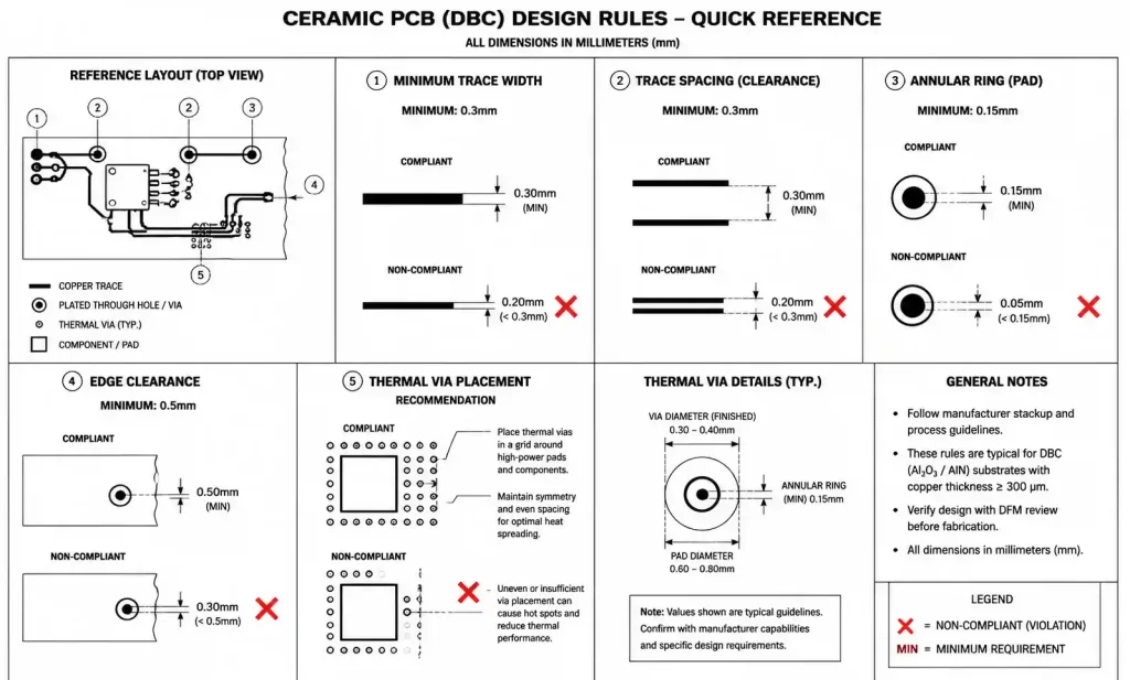
Minimum Feature Sizes and Design Rules
DBC process limitations determine minimum trace width, spacing, and via dimensions. For 0.3 mm copper on alumina or AlN:
- Minimum trace width: 0.3 mm (standard), 0.2 mm (advanced process)
- Minimum trace spacing: 0.3 mm (standard), 0.25 mm (advanced)
- Minimum pad annular ring: 0.15 mm
- Copper-to-edge clearance: 0.5 mm minimum
These constraints affect RF impedance matching and high-current power distribution. A 50-ohm microstrip on 0.635 mm alumina (Dk 9.8) with 0.3 mm copper requires approximately 0.45 mm trace width, which is achievable with standard DBC. However, differential pair routing for high-speed signals requires tight coupling (< 0.2 mm gap), which pushes toward AMB or thin-film processes.
Thermal Via Design
Unlike FR4 PCBs with plated through-holes, ceramic substrates use filled vias or thermal vias that connect top copper to bottom copper through laser drilling and metallization. Via diameter typically ranges from 0.3–0.5 mm with 0.1 mm copper plating thickness. For optimal thermal performance, place vias directly under high-power devices with 0.5–0.8 mm pitch.
Thermal via resistance depends on via diameter, plating thickness, and substrate thickness. A 0.4 mm diameter via through 0.635 mm alumina substrate with 0.1 mm copper plating provides approximately 8 K/W thermal resistance. For a 10W device, you need roughly 15–20 vias to achieve < 0.5 K/W via-contributed thermal resistance.
Edge Quality and Singulation
Ceramic substrates are brittle and prone to edge chipping during singulation. Laser scribing followed by mechanical breaking provides the cleanest edges. Leave at least 1.0 mm between active circuitry and board edge to prevent micro-cracks from propagating into the circuit area. For high-voltage applications (> 500V), increase edge clearance to 2.0 mm and specify edge rounding to eliminate sharp corners that concentrate electric fields.
6. Cost vs Performance Trade-offs in Ceramic PCB Selection
Material Cost Impact
Raw material cost follows a clear hierarchy: 96% alumina (baseline), 99.6% alumina (+30%), aluminum nitride (+350% to +450%), beryllium oxide (+1100% to +1400%). These cost multipliers apply to substrate material only. Total module cost includes copper metallization, assembly processes, and yield losses, which partially dilute the substrate cost premium.
For a 50 mm × 50 mm DBC substrate with 0.3 mm copper, representative pricing: 96% alumina $8–12, AlN $40–55, BeO $120–150 (quantities of 1000 pieces). At these prices, AlN adds $30–45 per module, which must be justified by performance improvements that enable higher power density, improved efficiency, or enhanced reliability.
Volume Considerations and Prototyping
Ceramic PCB fabrication requires specialized tooling and processes, leading to high NRE (non-recurring engineering) costs for prototypes. First article samples for a new design typically cost 10–20× production pricing. Plan for prototype iterations using the same substrate material as production to validate thermal and electrical performance accurately.
For volumes below 500 pieces annually, consider whether MCPCB (metal core PCB) with insulated metal substrate (IMS) technology can meet thermal requirements at lower cost. MCPCB with 3–5 W/m·K thermal conductivity works for many LED and power electronics applications where ceramic’s extreme performance is unnecessary.
Performance Optimization to Reduce Material Cost
Before committing to expensive AlN substrates, optimize thermal design using alumina:
- Increase copper thickness from 0.3 mm to 0.4 mm to improve lateral heat spreading (+15% cost)
- Add thermal vias under high-power devices to reduce thermal resistance by 20–30%
- Optimize die attach material (use high-thermal-conductivity solder or sintered silver)
- Improve heat sink interface with thermal interface materials (TIM) having < 0.5 K·cm²/W resistance
These optimizations add 15–25% to module cost but often avoid the 350% cost jump to AlN. Run thermal simulations comparing optimized alumina design against baseline AlN design. If junction temperature difference is < 10°C, the alumina solution likely offers better value.
Total Cost of Ownership
Consider lifecycle costs beyond initial substrate material. Higher junction temperatures from inadequate thermal management reduce MTBF (mean time between failures) and increase warranty costs. For automotive applications with 15-year life requirements, the incremental cost of AlN substrates may be recovered through reduced field failure rates and lower warranty exposure.
Similarly, for telecommunications infrastructure with 20-year design life, paying 4× substrate cost to reduce operating temperature by 20°C can improve system reliability from 99.9% to 99.99%, reducing expensive service calls and downtime penalties.
7. FAQ
What is the main difference between alumina and aluminum nitride PCB substrates?
The primary difference is thermal conductivity: aluminum nitride (170 W/m·K) conducts heat seven times better than 96% alumina (24 W/m·K). This allows AlN to manage higher power densities in smaller footprints. However, AlN costs 4–5× more than alumina. Electrically, both materials provide excellent insulation (> 10¹³ Ω·cm) and similar dielectric constants (8.9–9.9). Choose AlN when heat flux exceeds 30 W/cm² or when junction temperature cannot be controlled with alumina.
How do I calculate the required thermal conductivity for my application?
Calculate heat flux (power dissipation / device area in W/cm²). For heat flux below 15 W/cm², standard alumina works. Between 15–30 W/cm², run thermal simulation comparing alumina and AlN against your maximum junction temperature spec. Above 30 W/cm², AlN is typically required. Also consider substrate thickness: thinner substrates reduce thermal resistance but sacrifice mechanical strength.
Can I mix different ceramic substrate materials in the same power module?
Technically possible but not recommended. Different substrate materials have different CTEs, causing thermomechanical stress at assembly interfaces. If cost constraints require mixing materials, use alumina for low-power sections and AlN only for high-power devices. Ensure mechanical attachment methods (screws, clips) accommodate differential thermal expansion without inducing excessive stress.
What are the design rules for copper traces on ceramic PCB substrates?
For DBC process with 0.3 mm copper: minimum trace width 0.3 mm, minimum spacing 0.3 mm, minimum annular ring 0.15 mm. Copper-to-edge clearance should be 0.5 mm minimum, increased to 2.0 mm for high-voltage applications (> 500V). AMB process allows finer features (0.2 mm trace/space) but costs more. Always consult your fabricator’s specific design guidelines before finalizing the layout.
Does ceramic PCB substrate choice affect signal integrity in RF designs?
Yes, both dielectric constant and loss tangent matter. Alumina’s Dk of 9.8 requires narrower traces for 50-ohm impedance compared to FR4. Loss tangent of 0.0003 (alumina) provides low insertion loss up to 40 GHz. AlN has similar Dk (8.9) but higher loss tangent (0.0010), making it less ideal for RF despite superior thermal properties. For RF above 20 GHz, prioritize low loss tangent over thermal conductivity unless power dissipation is extreme.
What thickness should I specify for aluminum nitride substrates?
Standard thicknesses are 0.380 mm, 0.635 mm, and 1.0 mm. For power electronics (IGBTs, MOSFETs), 0.635 mm provides the best balance of thermal performance, mechanical strength, and cost. Use 0.380 mm only when package height is severely constrained and mechanical support is adequate. Thicker 1.0 mm substrates improve mechanical robustness for large modules (> 100 mm × 100 mm) but increase thermal resistance and cost.
Are there environmental or safety concerns with ceramic PCB materials?
Alumina and aluminum nitride are chemically stable and non-toxic in solid form. Standard occupational safety practices apply during machining (dust control). Beryllium oxide is toxic in powder form and requires specialized handling: HEPA filtration during machining, protective equipment, and beryllium-specific disposal procedures. BeO use is restricted to applications where no alternative meets performance requirements, primarily aerospace and defense.
How does ceramic PCB substrate cost compare to MCPCB or IMS technology?
Ceramic substrates cost 5–10× more than aluminum-based MCPCB with insulated metal substrate (IMS). However, ceramic provides superior thermal performance (24–180 W/m·K vs 3–5 W/m·K for IMS) and higher operating temperature (> 200°C vs 140°C for IMS). Use IMS for cost-sensitive LED and power electronics below 3W per device. Switch to ceramic when thermal requirements exceed IMS capability or when operating temperature exceeds 150°C.
8. Conclusion and Next Steps
Ceramic PCB substrate selection hinges on three factors: thermal management requirements, electrical performance specifications, and cost constraints. Alumina (Al2O3) serves as the baseline choice for most power electronics and RF applications up to 10 GHz, offering proven reliability and reasonable cost. Aluminum nitride (AlN) becomes necessary when heat flux exceeds 30 W/cm² or when CTE matching to silicon or GaN devices improves power cycling reliability. Beryllium oxide provides the ultimate performance but is restricted by handling requirements to specialized applications.
For your next design, start with thermal simulation to determine whether alumina can meet junction temperature requirements. If thermal resistance exceeds your budget by less than 30%, explore design optimizations (copper thickness, thermal vias, improved TIM) before upgrading to AlN. For RF applications, prioritize low loss tangent and stable dielectric properties, where alumina performs well up to 40 GHz.
Submit your Gerber files and thermal requirements for a free DFM review and substrate recommendation. Our applications engineers can run thermal simulations comparing alumina and AlN options, helping you select the most cost-effective solution that meets your performance and reliability requirements.