Skip to content
Andwin Circuits
  • Home
  • ProductsExpand
    • HDI multilayer PCB
    • Rigid Flex PCB
    • Flex pcb
    • Special PCBExpand
      • High Frequency PCBExpand
        • Rogers RO4350B PCB
        • Rogers RO4003 pcb
        • Rogers RO3003 PCB
        • Rogers 5880 PCB
        • DICLAD 527 PCB
        • Taconic TLX series
        • Taconic TLX-8 RF PCB
        • Taconic TLX-9 RF PCB
      • High speed pcbExpand
        • Megtron 6 High Speed PCB
        • TU-872 SLK Sp High Speed
      • High TG PCBExpand
        • SHENGYI SH260 PCB
        • ISOLA 370HR PCB
        • ISOLA IS410 PCB
        • ISOLA IS420 PCB
      • Heavy copper PCB
      • Copper coin pcb
      • Copper inlay PCB
    • Metal Core PCBExpand
      • Copper core pcb
      • Aluminum PCB
      • 2 Layers Aluminum PCB
      • Direct thermal MCPCB
      • 2 Layers Direct Thermal
    • Ceramic PCBExpand
      • DPC ceramic PCB
      • DBC ceramic PCB
      • Thick film Ceramic PCB
      • Al2O3 Alumina PCB
      • AIN ALN ceramic PCB
      • IGBT Ceramic PCB
  • ServiceExpand
    • PCB Assembly
    • Quick turn PCB assembly
    • PCBA conformal coating
  • IndustryExpand
    • Telecommunication
    • IoT and Wireless
    • Industrial Control
    • Thermal management
    • Power and Energy
    • IC test board
    • Automative
    • Medical
  • CapabilityExpand
    • Rigid PCB
    • Rigid flex PCB
    • Metal core PCB
    • PCB Assembly
  • TechnologyExpand
    • Blogs
    • Via in pad
    • PCB E-test
    • PCB stack up
    • MCPCB panelization
    • Controlled impedance PCB
  • AboutExpand
    • About us
    • Certification
    • Factory Tour
  • Contact
Andwin Circuits

1.what is HDI pcb

HDI is the abbreviation of High Density Interconnector.

High-density interconnect (HDI) manufacturing type printed circuit board, printed circuit board is a structural component formed by insulating materials supplemented with conductor wiring.

When the printed circuit board is made into a final product, integrated circuits, transistors (transistors, diodes), passive components (such as resistors, capacitors, connectors, etc.) and various other electronic parts will be installed on it.

With the help of wires, electronic signal connections and functions can be formed. Therefore, the printed circuit board is a platform that provides component connections and is used to receive the base of the connecting parts.

2.Manufacturing process and application fields of HDI multilayer PCB

Manufacturing process and application fields of HDI multilayer PCB are an indispensable part of modern electronic engineering.

HDI (high density interconnect) multilayer PCB is an advanced printed circuit board technology designed to meet the needs of increasingly complex and miniaturized electronic devices. Its manufacturing process involves multiple key steps, each of which requires highly precise and professional technical support.
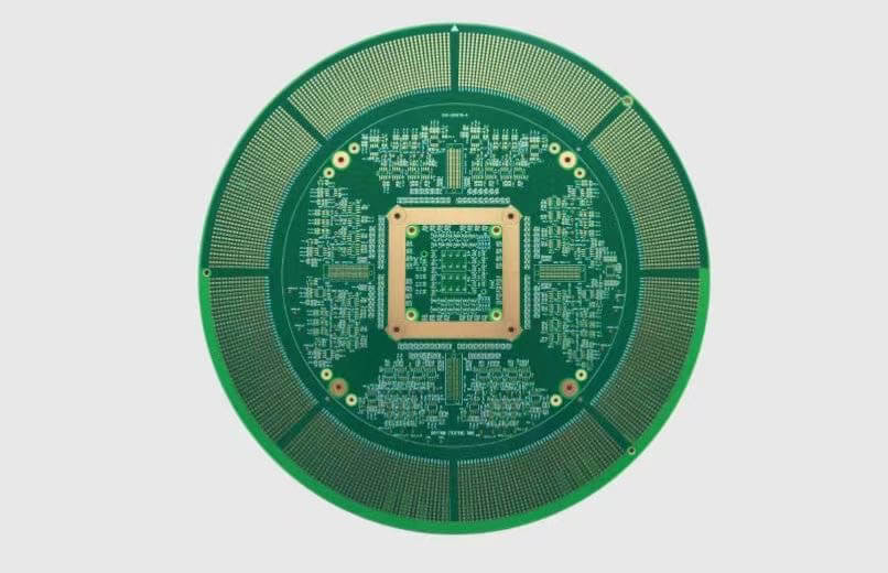
HDI multilayer PCB

First, the manufacturing of HDI multilayer PCB begins with the design stage. Design engineers use computer-aided design (CAD) software to create detailed circuit diagrams and layouts. These design files are then converted into manufacturing files to guide the subsequent production process. Next, the manufacturer selects a suitable substrate, usually FR4 or other high-performance materials, to ensure the stability and reliability of the circuit board.

After the substrate is ready, the manufacturing process enters the drilling and plating stage. HDI multilayer PCBs usually use laser drilling technology to achieve tiny apertures and high precision. These microvias (vias) are the core of HDI technology, allowing higher circuit density and more complex interconnect structures. Subsequently, through the electroplating process, these microvias are filled with conductive materials to ensure the smooth transmission of electrical signals.

Next, the etching of the circuit pattern is a key step. Through photolithography and chemical etching processes, the circuit pattern is accurately transferred to the substrate. This process requires highly precise control to ensure that the width and spacing of each circuit path meet the design requirements. Then, the lamination process presses multiple circuit layers together to form a multi-layer structure. Each layer is pre-impregnated with resin and treated with high temperature and high pressure to ensure the strong bonding and electrical performance between the layers.

After the lamination is completed, the HDI multi-layer PCB also needs surface treatment, such as gold plating or tin plating, to improve the welding performance and anti-oxidation ability. Finally, the circuit board undergoes rigorous testing and quality control to ensure that it meets the design specifications and performance requirements.
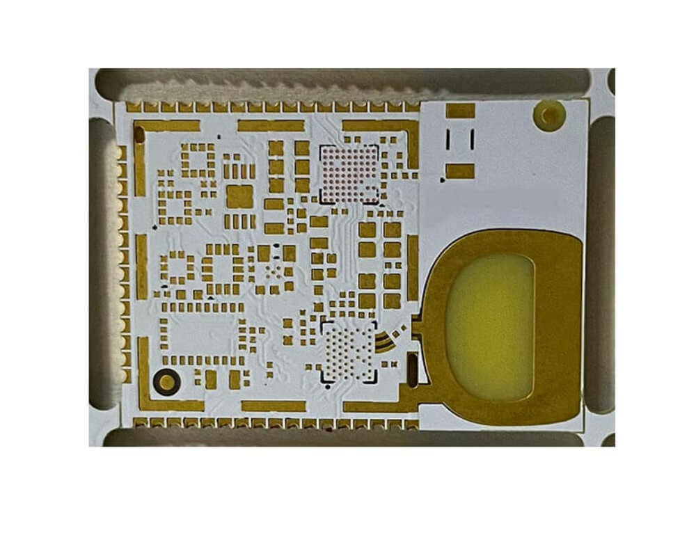
Metal core PCB

  • >Metal Core PCB
  • >Copper core pcb
  • >Aluminum PCB
  • ->2 Layers aluminum pcb
  • ->1500mm aluminum pcb
  • >Direct thermal MCPCB
  • ->2 Layers DTP MCPCB
  • Heavy copper PCB
  • Ceramic PCB
Get quote now ! |

Get professional one stop PCB solution from us!

Contact us now |

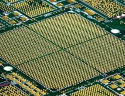
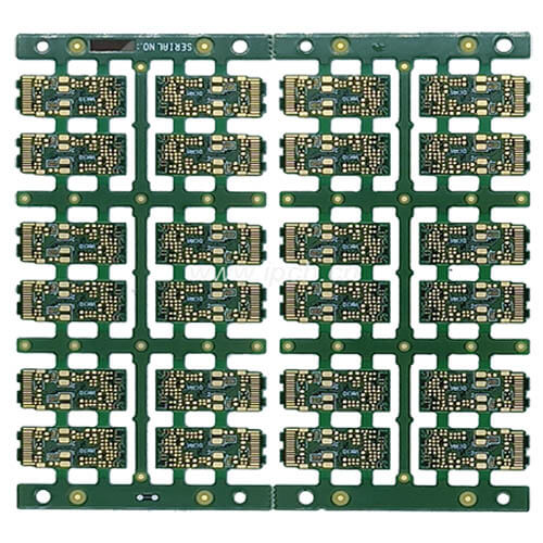
The application fields of HDI multi-layer PCBs

  • smartphones
  • tablets
  • laptops
  • automotive electronics,
  • aerospace
  • military fields

Contact us for your quote now!

Please send email: sales@andwinpcb.com ( priority ) with your PCB Gerber file Or/and BOM file to us,
Our teams will quote for you as soon as possible.

Or submit follow form our team will contact you soon.

Fill out my online form.

Address

Andwin Circuits Co.,Limited
Email: sales@andwinpcb.com
Tel: +86 755 2832 9394
Fax:+86 755 2992  6717
ADD:1-2F-1217,HouDeQun Industrial park,
NanTing RD NO.56,ShaJing,BaoAn,Shenzhen 518104,GuangDong,China

Products

  • HDI Multilayer PCB
  • Rigid Flex PCB
  • Flex pcb
  • High Frequency PCB
  • High speed pcb
  • Heavy copper PCB
  • Metal Core PCB
  • Ceramic PCB

Technology

  • Blogs
  • Via in pad
  • PCB E-test
  • PCB stack up
  • Metal core PCB panelization
  • Controlled impedance PCB

CERTIFICATION

Certification >>


Copyright© 2003 - 2026 Andwin | All Rights Reserved | Powered by Andwin

Scroll to top
  • Home
  • Products
    • HDI multilayer PCB
    • Rigid Flex PCB
    • Flex pcb
    • Special PCB
      • High Frequency PCB
        • Rogers RO4350B PCB
        • Rogers RO4003 pcb
        • Rogers RO3003 PCB
        • Rogers 5880 PCB
        • DICLAD 527 PCB
        • Taconic TLX series
        • Taconic TLX-8 RF PCB
        • Taconic TLX-9 RF PCB
      • High speed pcb
        • Megtron 6 High Speed PCB
        • TU-872 SLK Sp High Speed
      • High TG PCB
        • SHENGYI SH260 PCB
        • ISOLA 370HR PCB
        • ISOLA IS410 PCB
        • ISOLA IS420 PCB
      • Heavy copper PCB
      • Copper coin pcb
      • Copper inlay PCB
    • Metal Core PCB
      • Copper core pcb
      • Aluminum PCB
      • 2 Layers Aluminum PCB
      • Direct thermal MCPCB
      • 2 Layers Direct Thermal
    • Ceramic PCB
      • DPC ceramic PCB
      • DBC ceramic PCB
      • Thick film Ceramic PCB
      • Al2O3 Alumina PCB
      • AIN ALN ceramic PCB
      • IGBT Ceramic PCB
  • Service
    • PCB Assembly
    • Quick turn PCB assembly
    • PCBA conformal coating
  • Industry
    • Telecommunication
    • IoT and Wireless
    • Industrial Control
    • Thermal management
    • Power and Energy
    • IC test board
    • Automative
    • Medical
  • Capability
    • Rigid PCB
    • Rigid flex PCB
    • Metal core PCB
    • PCB Assembly
  • Technology
    • Blogs
    • Via in pad
    • PCB E-test
    • PCB stack up
    • MCPCB panelization
    • Controlled impedance PCB
  • About
    • About us
    • Certification
    • Factory Tour
  • Contact
Search