
Skip to content
Andwin Circuits
  • Home
  • ProductsExpand
    • HDI multilayer PCB
    • Rigid Flex PCB
    • Flex pcb
    • Special PCBExpand
      • High Frequency PCBExpand
        • Rogers RO4350B PCB
        • Rogers RO4003 pcb
        • Rogers RO3003 PCB
        • Rogers 5880 PCB
        • DICLAD 527 PCB
        • Taconic TLX series
        • Taconic TLX-8 RF PCB
        • Taconic TLX-9 RF PCB
      • High speed pcbExpand
        • Megtron 6 High Speed PCB
        • TU-872 SLK Sp High Speed
      • High TG PCBExpand
        • SHENGYI SH260 PCB
        • ISOLA 370HR PCB
        • ISOLA IS410 PCB
        • ISOLA IS420 PCB
      • Heavy copper PCB
      • Copper coin pcb
      • Copper inlay PCB
    • Metal Core PCBExpand
      • Copper core pcb
      • Aluminum PCB
      • 2 Layers Aluminum PCB
      • Direct thermal MCPCB
      • 2 Layers Direct Thermal
    • Ceramic PCBExpand
      • DPC ceramic PCB
      • DBC ceramic PCB
      • Thick film Ceramic PCB
      • Al2O3 Alumina PCB
      • AIN ALN ceramic PCB
      • IGBT Ceramic PCB
  • ServiceExpand
    • PCB Assembly
    • Quick turn PCB assembly
    • PCBA conformal coating
  • IndustryExpand
    • Telecommunication
    • IoT and Wireless
    • Industrial Control
    • Thermal management
    • Power and Energy
    • IC test board
    • Automative
    • Medical
  • CapabilityExpand
    • Rigid PCB
    • Rigid flex PCB
    • Metal core PCB
    • PCB Assembly
  • TechnologyExpand
    • Blogs
    • Via in pad
    • PCB E-test
    • PCB stack up
    • MCPCB panelization
    • Controlled impedance PCB
  • AboutExpand
    • About us
    • Certification
    • Factory Tour
  • Contact
Andwin Circuits
Home / Crosstalk Mitigation in High-Speed PCB Design

Crosstalk Mitigation in High-Speed PCB Design

ByGrace May 30, 2025May 27, 2025

Abstract

With the increasing demand for high-speed digital circuits, crosstalk has become a critical challenge in printed circuit board (PCB) design. Crosstalk introduces unwanted signal interference, leading to data corruption, timing errors, and reduced signal integrity. This paper explores the mechanisms of crosstalk in high-speed PCBs, analyzes its impact on signal integrity, and presents effective mitigation techniques. Key strategies include proper trace routing, impedance control, shielding, and advanced simulation tools. By implementing these methods, designers can minimize crosstalk and enhance the performance of high-speed electronic systems.

1. Introduction

As modern electronic devices operate at higher frequencies and faster data rates, PCB designs must address signal integrity (SI) challenges, particularly crosstalk. Crosstalk occurs when electromagnetic coupling between adjacent traces induces unwanted noise, degrading signal quality. In high-speed designs, where rise times are short and trace densities are high, crosstalk can significantly impact system reliability.

This paper discusses:

  • The fundamentals of crosstalk in PCBs.
  • Types of crosstalk (capacitive and inductive coupling).
  • Key factors influencing crosstalk.
  • Best practices for crosstalk reduction.
Contact us for PCB quote now |

2. Understanding Crosstalk in High-Speed PCBs

2.1 Definition and Types of Crosstalk

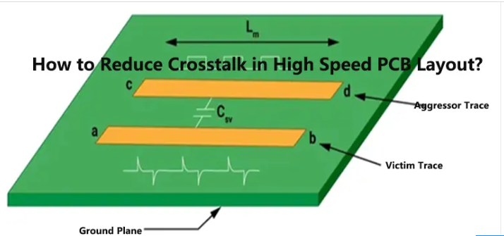
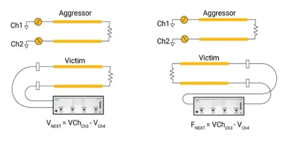
Crosstalk is the unwanted coupling of energy between two or more transmission lines. It is classified into two types:

  1. Near-End Crosstalk (NEXT) – Occurs when the interfering signal travels in the opposite direction to the victim signal.
  2. Far-End Crosstalk (FEXT) – Occurs when the interfering signal travels in the same direction as the victim signal.

Crosstalk arises from two primary coupling mechanisms:

  • Capacitive Coupling: Due to electric fields between adjacent traces.
  • Inductive Coupling: Due to magnetic fields generated by current flow.

2.2 Factors Influencing Crosstalk

Several factors contribute to crosstalk in high-speed PCBs:

  • Trace Spacing: Closer traces increase coupling.
  • Parallel Trace Length: Longer parallel sections enhance crosstalk.
  • Signal Rise Time: Faster edges (shorter rise times) increase high-frequency coupling.
  • Impedance Mismatch: Poorly matched traces reflect energy, worsening crosstalk.
  • Reference Plane Discontinuities: Gaps in ground/power planes increase coupling.

3. Techniques for Crosstalk Mitigation

3.1 Optimal Trace Routing

  • Increase Spacing: Follow the 3W rule (keep trace spacing ≥ 3× the trace width).
  • Minimize Parallel Lengths: Avoid long parallel runs between sensitive signals.
  • Use Differential Pair Routing: Balanced differential signals reject common-mode noise.

3.2 Impedance Control and Termination

  • Maintain consistent impedance to prevent reflections.
  • Use series termination resistors to dampen ringing.

3.3 Shielding and Grounding Techniques

  • Ground Guard Traces: Place grounded traces between high-speed signals.
  • Shielded Routing: Use microstrip/stripline configurations with solid reference planes.

3.4 Layer Stackup Optimization

  • Route high-speed signals between solid ground/power planes.
  • Avoid splitting reference planes under critical traces.

3.5 Advanced Simulation and Analysis

  • Use electromagnetic (EM) simulation tools (e.g., Ansys HFSS, Cadence Sigrity) to predict crosstalk.
  • Perform time-domain reflectometry (TDR) analysis for impedance verification.
Contact us for PCB quote now |

4. Case Study: Crosstalk Reduction in a DDR4 Memory Interface

A DDR4 memory bus operating at 3200 Mbps was experiencing crosstalk-induced bit errors. By applying:

  • Increased trace spacing (4W rule).
  • Shorter parallel lengths.
  • Improved ground plane continuity.
    The crosstalk noise was reduced by 40%, ensuring stable operation.

5. Conclusion

Crosstalk is a major concern in high-speed PCB design, but it can be effectively managed through proper layout techniques, impedance control, shielding, and simulation. By implementing these strategies, designers can achieve robust signal integrity and reliable high-speed performance.

Contact us for PCB quote now |
Post Tags: #aluminum clad pcb#aluminum core pcb#aluminum pcb#high-speed pcb

Post navigation

Previous Previous
Placing DC/DC Regulators on PCB Backside to Free Up Space for Digital ICs on Frontside
NextContinue
The Impact of PCB Characteristics on Power Distribution Network (PDN) Performance

Search

Search

Products

  • HDI Multilayer PCB
  • Rigid Flex PCB
  • Flex pcb
  • High Frequency PCB
  • High speed pcb
  • Heavy copper PCB
  • Metal Core PCB
  • Ceramic PCB

Address

Andwin Circuits Co.,Limited
Email: sales@andwinpcb.com
Tel: +86 755 2832 9394
Fax:+86 755 2992  6717
ADD:1-2F-1217,HouDeQun Industrial park,
NanTing RD NO.56,ShaJing,BaoAn,Shenzhen 518104,GuangDong,China

Products

  • HDI Multilayer PCB
  • Rigid Flex PCB
  • Flex pcb
  • High Frequency PCB
  • High speed pcb
  • Heavy copper PCB
  • Metal Core PCB
  • Ceramic PCB

Technology

  • Blogs
  • Via in pad
  • PCB E-test
  • PCB stack up
  • Metal core PCB panelization
  • Controlled impedance PCB

CERTIFICATION

Certification >>


Copyright© 2003 - 2026 Andwin | All Rights Reserved | Powered by Andwin

Scroll to top
  • Home
  • Products
    • HDI multilayer PCB
    • Rigid Flex PCB
    • Flex pcb
    • Special PCB
      • High Frequency PCB
        • Rogers RO4350B PCB
        • Rogers RO4003 pcb
        • Rogers RO3003 PCB
        • Rogers 5880 PCB
        • DICLAD 527 PCB
        • Taconic TLX series
        • Taconic TLX-8 RF PCB
        • Taconic TLX-9 RF PCB
      • High speed pcb
        • Megtron 6 High Speed PCB
        • TU-872 SLK Sp High Speed
      • High TG PCB
        • SHENGYI SH260 PCB
        • ISOLA 370HR PCB
        • ISOLA IS410 PCB
        • ISOLA IS420 PCB
      • Heavy copper PCB
      • Copper coin pcb
      • Copper inlay PCB
    • Metal Core PCB
      • Copper core pcb
      • Aluminum PCB
      • 2 Layers Aluminum PCB
      • Direct thermal MCPCB
      • 2 Layers Direct Thermal
    • Ceramic PCB
      • DPC ceramic PCB
      • DBC ceramic PCB
      • Thick film Ceramic PCB
      • Al2O3 Alumina PCB
      • AIN ALN ceramic PCB
      • IGBT Ceramic PCB
  • Service
    • PCB Assembly
    • Quick turn PCB assembly
    • PCBA conformal coating
  • Industry
    • Telecommunication
    • IoT and Wireless
    • Industrial Control
    • Thermal management
    • Power and Energy
    • IC test board
    • Automative
    • Medical
  • Capability
    • Rigid PCB
    • Rigid flex PCB
    • Metal core PCB
    • PCB Assembly
  • Technology
    • Blogs
    • Via in pad
    • PCB E-test
    • PCB stack up
    • MCPCB panelization
    • Controlled impedance PCB
  • About
    • About us
    • Certification
    • Factory Tour
  • Contact
Search