
Detailed Debugging Steps for Bluetooth PCB Antenna
Introduction
Bluetooth technology is widely used in wireless communication, and the performance of a Bluetooth device heavily depends on the efficiency of its PCB (Printed Circuit Board) antenna. Proper antenna design and debugging are crucial to achieving optimal signal strength, range, and reliability. This article provides a step-by-step guide to debugging a Bluetooth PCB antenna, covering key aspects such as impedance matching, radiation pattern optimization, and performance testing.
1. Understanding Bluetooth PCB Antenna Basics
Before diving into debugging, it’s essential to understand the fundamental principles of Bluetooth PCB antennas:
- Frequency Band: Bluetooth operates at 2.4 GHz (ISM band), requiring careful antenna tuning.
- Antenna Types: Common PCB antennas include Inverted-F (IFA), Monopole, Meandered, and Ceramic Chip Antennas.
- Impedance Matching: The antenna should be matched to 50 Ω to minimize reflections and maximize power transfer.
- Ground Plane Effects: The PCB’s ground plane size and shape significantly impact antenna performance.
2. Required Tools for Debugging
To debug a Bluetooth PCB antenna effectively, the following tools are necessary:
- Vector Network Analyzer (VNA) – Measures S-parameters (S11 for return loss).
- Spectrum Analyzer – Evaluates radiated power and frequency spectrum.
- Near-Field Probe – Detects electromagnetic interference (EMI) and radiation patterns.
- Impedance Matching Network Components (e.g., capacitors, inductors).
- RF Simulation Software (e.g., ANSYS HFSS, CST, or Altium Designer).
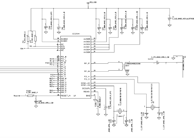
3. Step-by-Step Debugging Process
Step 1: Verify Antenna Design and Layout
Before fabrication, ensure the antenna design follows best practices:
- Trace Width & Length: Matches the required resonant frequency.
- Clearance: Maintain sufficient distance from other components to avoid detuning.
- Ground Plane: Ensure a solid ground reference beneath the antenna (if required).
Debugging Tip: If the antenna performance is poor, check for unintended coupling with nearby traces or components.
Step 2: Measure Return Loss (S11) Using a VNA
The return loss (S11) indicates how much power is reflected back due to impedance mismatch.
- Connect the VNA to the antenna feed point.
- Set the frequency range to 2.4–2.485 GHz.
- Analyze S11:
- Good Performance: S11 < –10 dB (90% power transfer).
- Poor Performance: S11 > –6 dB (requires tuning).
Debugging Tip: If S11 is high, adjust the matching network (LC components) or modify the antenna length.
Step 3: Tune the Impedance Matching Network
The antenna must be matched to 50 Ω for optimal power transfer.
- Use a Smith Chart (VNA feature) to visualize impedance.
- Add Series/Shunt Components:
- If impedance is too high (inductive), add a series capacitor or shunt inductor.
- If impedance is too low (capacitive), add a series inductor or shunt capacitor.
- Re-measure S11 after each adjustment.
Debugging Tip: Start with a pi-network (L-C-L) for flexible tuning.
Step 4: Check Radiation Pattern & Efficiency
A well-designed antenna should have an omnidirectional radiation pattern for Bluetooth applications.
- Use a near-field probe to scan the antenna’s radiation.
- Compare with simulation results (if available).
- Identify weak spots (e.g., nulls in radiation).
Debugging Tip: If radiation is directional, modify the ground plane or antenna shape.
Step 5: Evaluate Real-World Performance
After tuning, test the antenna in real-world conditions:
- Range Test: Measure the maximum communication distance.
- Interference Test: Check for signal degradation near Wi-Fi routers or other 2.4 GHz devices.
- Throughput Test: Verify data transfer stability.
Debugging Tip: If range is poor, check for PCB losses, shielding issues, or incorrect antenna polarization.
Step 6: Fine-Tune with EMI/EMC Considerations
Bluetooth devices must comply with EMI/EMC regulations (FCC, CE).
- Use a spectrum analyzer to detect spurious emissions.
- Add ferrite beads or shielding if excessive noise is present.
- Ensure harmonics are within acceptable limits.
Debugging Tip: If EMI is high, optimize the ground plane or add decoupling capacitors.
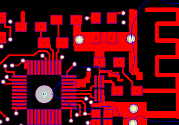
4. Common Issues and Solutions
| Issue | Possible Cause | Solution |
|---|---|---|
| High S11 (> –6 dB) | Impedance mismatch | Adjust matching network |
| Weak signal strength | Poor radiation efficiency | Optimize antenna geometry |
| Frequency shift | Incorrect trace length | Recalculate antenna dimensions |
| EMI interference | Poor grounding | Improve ground plane |
5. Final Validation
Before mass production, conduct:
- Long-term stability tests.
- Environmental tests (temperature, humidity).
- Certification testing (FCC, Bluetooth SIG).
Conclusion
Debugging a Bluetooth PCB antenna requires systematic testing and optimization. By following these steps—measuring S11, tuning impedance, verifying radiation patterns, and testing real-world performance—engineers can ensure reliable Bluetooth connectivity. Proper debugging minimizes signal loss, maximizes range, and ensures compliance with regulatory standards.
By applying these techniques, designers can achieve optimal Bluetooth antenna performance in their PCB designs.