Eight Essential Steps to Set Up PCB Constraints
Introduction
Printed Circuit Board (PCB) design is a complex process that requires careful planning and precise execution. One of the most critical aspects of PCB design is setting up constraints to ensure signal integrity, manufacturability, and reliability. Constraints define the rules that govern trace widths, spacing, via sizes, and other design parameters.
In this article, we will explore the eight essential steps to properly set up PCB constraints, ensuring a smooth and error-free design process.
Step 1: Define Design Requirements
Before setting constraints, it is crucial to understand the design requirements:
- Electrical Requirements: Signal speed, impedance control, and power delivery needs.
- Mechanical Requirements: Board size, layer stack-up, and component placement restrictions.
- Manufacturing Constraints: Minimum trace width, drill sizes, and solder mask clearances.
Gathering these details early helps in setting accurate constraints that align with the PCB’s functionality and fabrication capabilities.
Step 2: Set Up the Layer Stack-Up
The PCB layer stack-up determines signal integrity and power distribution. Key considerations include:
- Number of Layers: High-speed designs may require multiple signal and ground layers.
- Material Selection: FR4, Rogers, or other substrates based on frequency and thermal needs.
- Impedance Control: Define dielectric thickness and trace width for controlled impedance signals (e.g., 50Ω for single-ended, 100Ω for differential pairs).
Most PCB design tools (e.g., Altium Designer, Cadence Allegro) allow stack-up configuration before applying constraints.
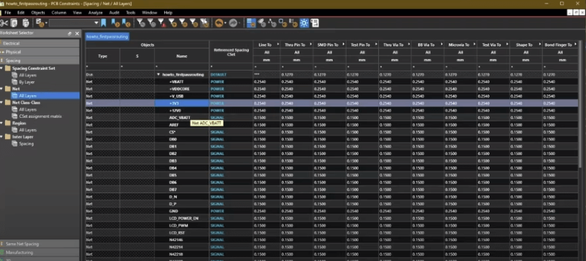
Step 3: Establish Electrical Constraints
Electrical constraints ensure signal integrity and prevent issues like crosstalk and EMI. Key settings include:
- Trace Width & Spacing:
- High-current traces need wider widths.
- High-speed signals require controlled impedance.
- Differential Pair Rules: Define coupling and length matching tolerances.
- Net Classes: Group nets (e.g., power, high-speed, analog) and assign specific rules.
Using net classes helps apply constraints efficiently across similar signal types.
Step 4: Configure Routing Constraints
Routing constraints guide how traces are placed and connected:
- Minimum/Maximum Trace Length: Critical for timing-sensitive signals (e.g., DDR, PCIe).
- Via Usage:
- Define via sizes (e.g., micro-vias for HDI designs).
- Set via stitching rules for ground/power planes.
- Routing Topology: Specify daisy-chain, star, or fly-by routing for buses.
Proper routing constraints prevent signal degradation and manufacturing issues.
Step 5: Set Spacing and Clearance Rules
Clearance rules prevent short circuits and ensure manufacturability:
- Trace-to-Trace Spacing: Avoid crosstalk, especially in dense layouts.
- Component-to-Component Clearance: Ensures assembly feasibility.
- Copper-to-Board Edge: Prevents delamination during fabrication.
Modern PCB tools support 3D clearance checks for complex designs.
Step 6: Define Manufacturing Constraints
Manufacturing constraints ensure the design can be reliably produced:
- Minimum Drill Size: Smaller vias increase cost; balance performance and budget.
- Solder Mask & Silkscreen Rules: Define openings and text sizes.
- Aspect Ratio: (Board thickness / smallest hole size) should be within fabricator limits (typically ≤ 10:1).
Consult your PCB manufacturer’s design guidelines before finalizing constraints.
Step 7: Apply High-Speed Design Rules
High-speed PCBs require additional constraints:
- Length Matching: Ensures synchronous signals arrive simultaneously.
- Controlled Impedance: Requires precise trace geometry and dielectric settings.
- Return Paths: Ensure uninterrupted ground planes beneath high-speed traces.
Simulation tools (e.g., HyperLynx, SIwave) help validate high-speed constraints.
Step 8: Validate Constraints with DRC (Design Rule Check)
Before finalizing the design, run a Design Rule Check (DRC) to ensure all constraints are met:
- Electrical Rule Check (ERC): Verifies unconnected nets and incorrect power ratings.
- Manufacturing Rule Check (MRC): Confirms drill sizes, spacing, and layer alignment.
- Signal Integrity Analysis: Simulates high-speed performance.
Fix any violations before proceeding to fabrication.
Conclusion
Setting up PCB constraints is a structured process that requires attention to electrical, mechanical, and manufacturing requirements. By following these eight steps—defining requirements, configuring stack-up, setting electrical and routing rules, managing clearances, applying high-speed rules, and validating with DRC—you can ensure a robust and manufacturable PCB design.
Proper constraint management reduces errors, speeds up production, and improves overall board reliability. Always collaborate with your fabrication house to align constraints with their capabilities, ensuring a smooth transition from design to production.
By mastering constraint setup, PCB designers can optimize performance, reduce costs, and accelerate time-to-market for electronic products.