Electronics PCB Manufacturing: Processes, Technologies, and Industry Trends
Introduction
Printed Circuit Boards (PCBs) are the foundation of modern electronics, serving as the platform for interconnecting electronic components and enabling the functionality of devices ranging from smartphones to industrial machinery. The manufacturing of PCBs is a complex and highly specialized process that involves multiple stages, from design and fabrication to assembly and testing. This article provides a comprehensive overview of electronics PCB manufacturing, covering the key processes, technologies, challenges, and future trends shaping the industry.
1. Overview of PCB Manufacturing
1.1 What is a PCB?
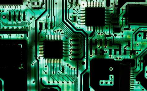
A PCB is a flat board made of insulating material (typically fiberglass or composite epoxy) with conductive pathways (traces) etched or printed onto its surface. These traces connect electronic components, such as resistors, capacitors, and integrated circuits (ICs), to form a functional circuit.
1.2 Types of PCBs
PCBs can be classified based on their structure and complexity:
- Single-Sided PCBs: Components and traces are on one side of the board.
- Double-Sided PCBs: Components and traces are on both sides, connected by vias.
- Multi-Layer PCBs: Consist of multiple layers of conductive traces separated by insulating layers.
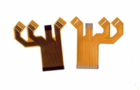
- Flexible PCBs: Made of flexible materials, allowing the board to bend or twist.
- Rigid-Flex PCBs: Combine rigid and flexible sections for complex designs.
2. Key Stages of PCB Manufacturing
The PCB manufacturing process involves several stages, each requiring precision and expertise.
2.1 Design and Layout
The process begins with the design of the PCB using Computer-Aided Design (CAD) software. Key considerations include:
- Schematic Design: Creating a circuit diagram that defines the connections between components.
- Component Placement: Arranging components to optimize performance and manufacturability.
- Trace Routing: Designing the conductive pathways that connect components.
- Design for Manufacturability (DFM): Ensuring the design can be efficiently and reliably manufactured.
2.2 PCB Fabrication
PCB fabrication involves transforming the design into a physical board. The key steps include:
2.2.1 Material Preparation
- Substrate Selection: Choosing the base material, typically FR-4 (fiberglass-reinforced epoxy).
- Copper Cladding: Laminating copper foil onto the substrate to create conductive layers.
2.2.2 Circuit Patterning
- Photolithography: Applying a photoresist layer, exposing it to UV light through a mask, and developing it to create the circuit pattern.
- Etching: Removing unwanted copper using chemical etchants, leaving behind the desired traces.
2.2.3 Layer Stacking (for Multi-Layer PCBs)
- Multiple layers of substrate and copper are stacked and bonded using heat and pressure.
2.2.4 Drilling
- Holes are drilled for vias (connections between layers) and through-hole components.
2.2.5 Plating
- The holes are plated with copper to create electrical connections between layers.
2.2.6 Surface Finishing
- Applying a surface finish (e.g., HASL, ENIG, OSP) to protect the copper and improve solderability.
2.2.7 Solder Mask and Silkscreen
- Applying a solder mask to insulate the traces and a silkscreen for labeling.
2.3 PCB Assembly
PCB assembly involves mounting components onto the fabricated board. The two primary methods are:
2.3.1 Surface Mount Technology (SMT)
- Solder Paste Application: Applying solder paste to the pads using a stencil.
- Component Placement: Using a pick-and-place machine to position SMD components.
- Reflow Soldering: Heating the board in a reflow oven to melt the solder paste and form solder joints.
2.3.2 Through-Hole Technology (THT)
- Component Insertion: Inserting THT components into drilled holes.
- Wave Soldering: Passing the board over a wave of molten solder to solder the component leads.
2.4 Testing and Inspection
After assembly, the PCB undergoes rigorous testing and inspection to ensure functionality and quality. Common methods include:
- Automated Optical Inspection (AOI): Detecting visual defects such as misaligned components or solder bridges.
- In-Circuit Testing (ICT): Verifying the electrical performance of individual components.
- Functional Testing: Ensuring the assembled PCB performs its intended function.

3. Technologies in PCB Manufacturing
3.1 Advanced Materials
- High-Frequency Materials: Used for high-speed and RF applications.
- Flexible Substrates: Enable the production of flexible and rigid-flex PCBs.
- Thermal Management Materials: Improve heat dissipation in high-power applications.
3.2 Automation and Industry 4.0
- Automated Machinery: Pick-and-place machines, AOI systems, and robotic soldering.
- IoT and Data Analytics: Real-time monitoring and optimization of production processes.
- AI and Machine Learning: Predictive maintenance and defect detection.
3.3 Additive Manufacturing
- 3D Printing: Used for prototyping and producing custom PCBs with complex geometries.
3.4 Laser Technology
- Laser Drilling: Precision drilling of microvias for high-density designs.
- Laser Direct Imaging (LDI): High-resolution patterning of circuit traces.
4. Challenges in PCB Manufacturing
4.1 Miniaturization
As electronic devices become smaller, PCB manufacturers must produce boards with finer traces, smaller components, and higher densities.
4.2 High-Speed and High-Frequency Designs
High-speed and RF applications require precise impedance control and advanced materials, increasing manufacturing complexity.
4.3 Thermal Management
High-power components generate significant heat, requiring effective thermal management solutions.
4.4 Environmental Regulations
Manufacturers must comply with environmental regulations, such as the Restriction of Hazardous Substances (RoHS) directive.
4.5 Supply Chain Disruptions
Component shortages and supply chain disruptions can delay production and increase costs.
5. Future Trends in PCB Manufacturing
5.1 High-Density Interconnect (HDI) PCBs
HDI PCBs feature finer traces, smaller vias, and higher component densities, enabling more compact and powerful devices.
5.2 Flexible and Stretchable Electronics
The demand for wearable devices and IoT applications is driving the development of flexible and stretchable PCBs.
5.3 Embedded Components
Embedding passive and active components within the PCB substrate reduces size and improves performance.
5.4 Green Manufacturing
Sustainable practices, such as using lead-free solder and recycling materials, are becoming more common.
5.5 Advanced Packaging
Technologies like 3D packaging and System-in-Package (SiP) are enabling higher performance and integration.
6. Choosing a PCB Manufacturer
When selecting a PCB manufacturer, consider the following factors:
- Capabilities: Ensure the manufacturer can handle your specific requirements, such as HDI or flexible PCBs.
- Quality Standards: Look for certifications like ISO 9001 and IPC-A-610.
- Turnaround Time: Choose a manufacturer that can meet your production deadlines.
- Cost: Compare pricing while considering the quality and reliability of the manufacturer.
- Customer Support: A responsive and supportive team can make the collaboration smoother.
Conclusion
Electronics PCB manufacturing is a complex and dynamic field that plays a critical role in the production of modern electronic devices. By leveraging advanced technologies, adhering to industry standards, and addressing challenges such as miniaturization and thermal management, manufacturers can produce high-quality PCBs that meet the demands of today’s rapidly evolving electronics industry. As the industry continues to advance, trends such as HDI PCBs, flexible electronics, and green manufacturing are shaping the future of PCB manufacturing. By staying informed and adopting best practices, manufacturers can drive innovation and deliver reliable, high-performance PCBs for a wide range of applications.