FPC Minimum Line Width/Spacing (0.05mm): Critical Design Guidelines for High-Density Applications (2026)
Here’s the reality of 0.05mm (50μm, ~2 mil) FPC design rules: they let you pack way more traces into tight spaces, but they’ll kill your yield if you don’t respect the manufacturing constraints. This guide covers when to use these fine lines, what it costs in terms of materials and process control, and how to keep your flex circuits reliable in dynamic bending areas.
What 0.05mm Trace Geometry Enables
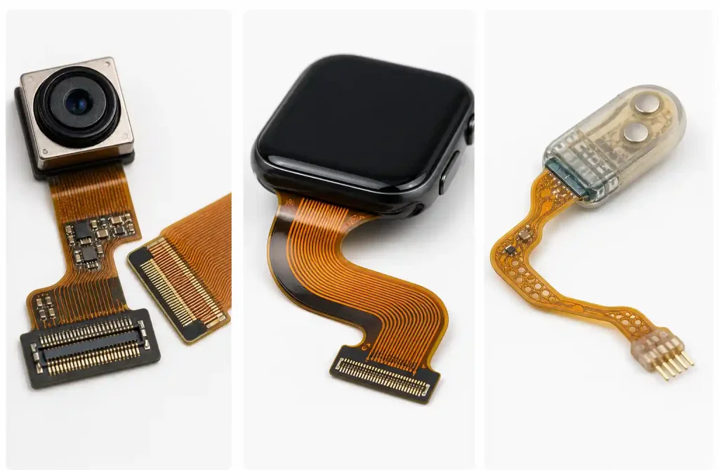
Fine-pitch FPCs with 0.05mm lines let you route between ultra-fine BGA pads (0.3mm pitch) or COF bonding pads that standard 0.1mm rules simply can’t handle. A smartphone camera module, for example, might need 40+ signals in a 5mm width. With 0.1mm traces, you’re forced to add layers; at 0.05mm, you can keep it single-sided or double-sided—saving cost and thickness.
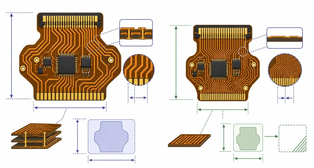
The catch? You need Laser Direct Imaging (LDI), precise etching control, and IPC-6013 Class 3 quality. Not every fab can reliably pull this off at volume.
Key Parameters That Govern Feasibility
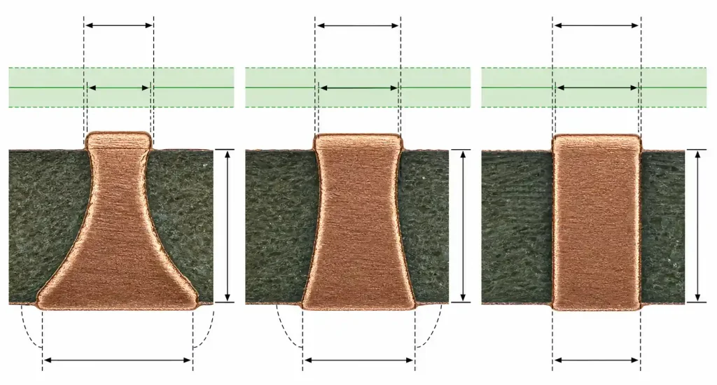
Copper Weight & Etch Profile: Stick with 0.5 oz (18μm) or 1/3 oz (12μm) copper. 1 oz copper with 0.05mm lines causes severe undercut during wet etching—you’ll get inconsistent trace widths and open circuits. With a modified semi-additive process (mSAP), target an etch factor of 2:1 to 3:1. For 18μm copper, expect 6-9μm of lateral undercut per side, so compensate in your Gerber artwork.
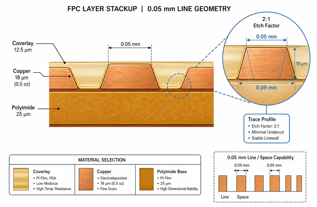
Base Material: Use 25μm or 12.5μm polyimide film with low CTE. Thicker films (50μm+) introduce registration errors during lamination, making it tough to hold 0.05mm tolerances across layers. Prefer adhesiveless or PSA constructions over traditional acrylic adhesive—acrylic squeezes out during lamination and bridges fine traces.
Design Rule Comparison: 0.05mm vs. Standard FPC
| Design Parameter | Standard FPC | Advanced FPC | Ultra-Fine FPC (0.05mm) | IPC Class |
|---|---|---|---|---|
| Min. trace width | 0.10 mm (4 mil) | 0.075 mm (3 mil) | 0.05 mm (2 mil) | Class 2/3 |
| Min. trace spacing | 0.10 mm (4 mil) | 0.075 mm (3 mil) | 0.05 mm (2 mil) | Class 2/3 |
| Copper weight | 0.5–1 oz | 0.5 oz | 0.5 oz / 1/3 oz | — |
| Via diameter (if rigid-flex) | 0.20 mm | 0.15 mm | 0.10 mm | — |
| Pad-to-trace clearance | 0.10 mm | 0.075 mm | 0.05 mm | Class 2/3 |
| Registration tolerance | ±0.10 mm | ±0.075 mm | ±0.05 mm | Class 3 |
| Patterning method | UV exposure | LDI | LDI or laser ablation | — |
Moving from 0.10mm to 0.05mm isn’t just about finer artwork—it demands tighter control across the whole fab process. Expect 2-3 week lead times for prototypes and higher NRE costs for first-article builds.
DFM Considerations: Where Designs Fail
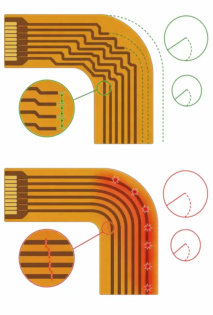
Traces Near Bend Areas: If you route 0.05mm pitch traces parallel to the bend axis, you’re asking for trouble. Dynamic flex regions (>1000 cycles) need increased spacing—at least 0.15mm—and a bend radius of 10× total FPC thickness (or 20× for repeated bending). Route perpendicular to the bend direction whenever possible.
Coverlay Registration: Traditional photoimageable coverlay can’t hold ±0.05mm registration reliably. A 0.03mm misalignment bridges adjacent traces. PSA coverlay or laser-cut polyimide works better, but costs more. Also watch for adhesive bleed from stiffeners—it can short fine-pitch circuits.
Yield & Cost Impact: Expect a 10-20% yield drop during early production at 0.05mm compared to 0.1mm designs. You’ll pay a 30-50% premium on piece-part pricing. If you only need fine lines in localized areas (e.g., connector breakout), use hybrid rules—0.05mm only where essential, 0.1mm elsewhere—to save cost.
When to Use 0.05mm Rules
Essential for: Smartphone camera modules, foldable display interconnects, TWS earbuds (<50mm² board space), implantable medical sensors, catheter electrode arrays, and AR/VR headsets where every micron counts.
Skip it if: Your routing fits in 0.1mm geometry. Industrial controls, non-ADAS automotive sensors, and LED lighting flex circuits rarely need 0.05mm and the cost premium isn’t worth it.
Material & Process Selection for 0.05mm FPC
| Material/Process | Specification | Impact on 0.05mm Design | Recommendation |
|---|---|---|---|
| Polyimide film | 12.5–25 μm thickness | Thinner films improve dimensional stability | Use 25 μm; 12.5 μm for extreme thinness |
| Copper foil | ED (electrodeposited) 0.5 oz | Fine grain supports narrow lines | Avoid rolled-annealed copper (grain size too large) |
| Adhesive | Adhesiveless or PSA | Eliminates squeeze-out risk | Avoid acrylic adhesive in fine-pitch areas |
| Patterning | LDI | ±15 μm registration accuracy | UV exposure can’t hold 0.05mm spacing |
| Etching | Spray/pulse control | Controls undercut <10 μm per side | Immersion etching too slow for production |
| Surface finish | ENIG (0.05–0.125μm Au) | Protects traces; maintains solderability | Avoid HASL; it bridges fine pads |
For high-reliability (automotive/medical), specify low-CTE polyimide (e.g., DuPont Kapton E) with adhesiveless construction. This minimizes thermal mismatch during assembly and keeps dynamic flex regions stable.
FAQ
What is the minimum bend radius for FPC with 0.05mm traces?
For static bending, use 10× total FPC thickness. For dynamic flexing (>1000 cycles), use 20× thickness and widen trace spacing to 0.15mm in the bend region to prevent copper fatigue cracking.
Can I use 0.05mm line width and spacing on multi-layer rigid-flex boards?
Yes, but only on the flexible layers. Rigid sections should stick to standard HDI rules (typically 0.1mm). Ensure layer-to-layer registration is ±0.05mm or better—this requires LDI imaging and Class 3 manufacturing.
How does 0.05mm geometry affect impedance control?
Narrow traces have higher characteristic impedance for a given dielectric thickness. For 50-ohm single-ended traces at 0.05mm width, you may need thinner dielectric (12.5μm) or lower-Dk materials. Use an impedance calculator and request TDR verification from your FPC manufacturer.
What is the cost difference between 0.05mm and 0.1mm FPC?
Prototype quantities (10–50 pcs) cost 40-60% more for 0.05mm due to lower yields and longer process times. At production volumes (>5K pcs), the premium drops to 20-30% as yields stabilize.
Which FPC manufacturers can reliably produce 0.05mm geometry?
Look for manufacturers with LDI capability, Class 3 IPC-6013 certification, and experience in smartphone or medical device supply chains. Request process capability data (Cpk values for line width/spacing) and first-article inspection reports before committing.
Do I need special DFM checks for 0.05mm FPC designs?
Yes. Check spacing violations near bend areas, coverlay-to-trace clearance, stiffener placement tolerance, and copper balancing across the panel. Most EDA tools have DFM rules calibrated for rigid PCBs—you may need custom rule sets for fine-pitch FPC.
Conclusion
0.05mm line width/spacing unlocks serious routing density, enabling smaller, lighter flexible circuits. But it comes with strict material constraints, tighter process control, and higher costs. Before specifying it across your whole design, ask yourself whether localized use in high-density areas can meet your needs while keeping the rest at 0.1mm rules—this hybrid approach balances performance and cost.
For your next FPC project, run a DFM review before finalizing Gerbers. Our CAM team can spot yield risks, suggest optimizations, and offer cost-effective alternatives without compromising functionality. Send your design files for a free manufacturability assessment.