What is High Frequency PCB?
Introduction to High Frequency PCBs
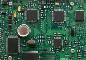
In today’s rapidly advancing electronic landscape, the demand for high-speed and high-frequency applications has grown exponentially. At the heart of these applications lies a critical component: the High Frequency Printed Circuit Board (PCB). These specialized circuit boards are engineered to handle signals in the microwave and radio frequency ranges, typically operating above 1 GHz, with some applications reaching into the millimeter-wave spectrum (30 GHz and beyond).
High frequency PCBs differ significantly from their conventional counterparts in terms of material composition, design considerations, and manufacturing processes. They are essential components in modern telecommunications, aerospace systems, military applications, medical equipment, and advanced computing systems where signal integrity at high frequencies is paramount.
Key Characteristics of High Frequency PCBs
1. Specialized Dielectric Materials
The foundation of any high frequency PCB is its dielectric material. Unlike standard FR-4 material used in conventional PCBs, high frequency boards utilize advanced substrates with carefully controlled electrical properties:
Low Dielectric Constant (Dk): Typically between 2.2 and 3.8, compared to FR-4’s 4.3-4.8
Low Dissipation Factor (Df): Usually below 0.004, minimizing signal loss
Consistency: Uniform dielectric properties across the entire board
Thermal Stability: Minimal variation in electrical properties with temperature changes
Common high-frequency materials include:
– PTFE-based materials (Teflon)
– Ceramic-filled PTFE composites
– Hydrocarbon ceramics
– Liquid Crystal Polymer (LCP)
– Polyimide for certain applications
2. Precise Impedance Control
Maintaining consistent characteristic impedance (typically 50Ω or 75Ω) is crucial in high frequency PCBs. This requires:
– Tight tolerances on trace widths and thicknesses
– Controlled dielectric thickness
– Careful consideration of the reference plane configuration
– Advanced modeling and simulation during design
3. Low Signal Loss
High frequency signals are particularly susceptible to various loss mechanisms:
Conductor Loss: Reduced through the use of smooth copper surfaces and proper plating
Dielectric Loss: Minimized by selecting appropriate substrate materials
Radiation Loss:Controlled through proper board design and shielding
4. Advanced Manufacturing Techniques
Fabricating high frequency PCBs requires specialized processes:
– Laser drilling for precise microvias
– Plasma treatment for surface preparation
– Tight control over etching processes
– Specialized plating techniques
– Advanced quality control measures
Design Considerations for High Frequency PCBs
1. Transmission Line Structures
Proper transmission line design is essential for maintaining signal integrity:
– Microstrip lines (signal trace on outer layer with ground plane beneath)
– Stripline (signal trace embedded between two ground planes)
– Coplanar waveguide (signal trace with adjacent ground planes on the same layer)
– Grounded coplanar waveguide (combines coplanar and microstrip features)
2. Via Design and Placement
Vias in high frequency PCBs present significant challenges:
– Stub effects that can cause signal reflections
– Impedance discontinuities
– Proper via fencing for shielding
– Back-drilling to remove unused via portions
3. EMI/EMC Considerations
High frequency circuits are particularly susceptible to electromagnetic interference:
– Proper grounding strategies
– Shielding techniques
– Careful component placement
– Filter implementation
4. Thermal Management
High frequency circuits often generate significant heat:
– Thermal via arrays
– Heat spreaders
– Careful material selection for thermal conductivity
– Consideration of coefficient of thermal expansion (CTE)
Applications of High Frequency PCBs
1. Telecommunications
– 5G infrastructure and devices
– Base station antennas
– Microwave communication systems
– Satellite communication equipment
2. Aerospace and Defense
– Radar systems
– Electronic warfare systems
– Avionics
– Satellite systems
3. Medical Equipment
– MRI machines
– Medical imaging systems
– Therapeutic equipment
– High-frequency surgical tools
4. Automotive
– Advanced driver assistance systems (ADAS)
– Vehicle-to-vehicle communication
– Radar-based collision avoidance systems
– In-vehicle networking
5. Industrial and Scientific
– RF identification (RFID) systems
– High-frequency test equipment
– Scientific instrumentation
– Industrial process control systems
Manufacturing Challenges and Solutions
1. Material Handling
High frequency materials often present handling challenges:
– PTFE materials are soft and require special processing
– Some materials have poor adhesion to copper
– Dimensional stability issues during processing
Solutions include:
– Specialized surface treatments
– Modified lamination processes
– Careful handling procedures
2. Copper Surface Roughness
Excessive copper roughness can increase conductor losses:
– Use of low-profile copper foils
– Advanced plating processes
– Surface treatment optimization
3. Plating Processes
Achieving consistent plating in high frequency applications:
– Pulse plating for uniform thickness
– Selective plating techniques
– Advanced plating chemistry control
4. Quality Control
Stringent testing requirements:
– Time-domain reflectometry (TDR) for impedance verification
– High-frequency network analysis
– Advanced automated optical inspection (AOI)
– Cross-section analysis
Future Trends in High Frequency PCBs
1. Higher Frequency Applications
With the push toward millimeter-wave and terahertz applications:
– Development of new substrate materials
– Advanced fabrication techniques for finer features
– Improved modeling and simulation tools
2. Integration with Advanced Packaging
– Embedded components
– 3D packaging solutions
– Heterogeneous integration
3. Sustainable Materials
– Development of eco-friendly high-frequency materials
– Recycling and reuse strategies
– Reduced hazardous substance compliance
4. AI in Design and Manufacturing
– Machine learning for design optimization
– AI-driven manufacturing process control
– Predictive maintenance for high-frequency PCB production
Conclusion
High frequency PCBs represent a critical enabling technology for modern electronic systems that operate at microwave and millimeter-wave frequencies. These specialized circuit boards require careful material selection, advanced design techniques, and precision manufacturing processes to ensure optimal performance in demanding applications.
As wireless communications continue to evolve toward higher frequencies and greater bandwidths, the importance of high frequency PCBs will only grow. Engineers and manufacturers must continue to innovate in materials, design methodologies, and fabrication techniques to meet the ever-increasing demands of high-speed electronic systems.
Understanding the principles and challenges of high frequency PCB technology is essential for anyone involved in the design, manufacture, or application of modern electronic systems where signal integrity at high frequencies is paramount. As we look to the future, advancements in this field will play a pivotal role in enabling next-generation technologies across telecommunications, computing, transportation, healthcare, and beyond.