High-Frequency Rigid-Flex PCB Selection Guide for 5G Base Station Construction
The global rollout of 5G infrastructure demands electronic components capable of operating at millimeter-wave frequencies while surviving harsh outdoor environments. High-frequency rigid-flex PCB technology has emerged as the critical enabling solution for modern base station designs, offering the dimensional stability of rigid boards combined with the spatial adaptability of flexible circuits. Research indicates that 5G networks require up to 10× more base stations than 4G LTE to achieve comparable coverage, placing enormous pressure on manufacturers to deliver compact, reliable RF interconnect solutions. This comprehensive guide analyzes the key selection criteria engineers must evaluate when specifying Rigid-flex PCB solutions for 5G macrocells, small cells, and massive MIMO antenna systems.
Quick Answer: High-frequency rigid-flex PCB for 5G base stations is a hybrid circuit board combining rigid and flexible substrates, engineered with low-loss dielectric materials to transmit signals above 6 GHz while withstanding thermal cycling, vibration, and environmental stress in telecommunications infrastructure.
Why This Guide Matters Now
The telecommunications industry stands at an inflection point. With 3GPP Release 18 introducing advanced antenna architectures and carrier aggregation schemes pushing bandwidth demands higher, the margin for error in PCB specification has effectively vanished. Selection decisions made today will determine whether base station designs can accommodate software-defined radio upgrades through the 2030 network lifecycle. This guide distills practical selection frameworks validated across multiple commercial 5G deployments, translating complex material science and electromagnetic theory into actionable engineering criteria.
The 5G Infrastructure Challenge
The Density Problem in Modern Base Stations
5G New Radio (NR) operates across frequency ranges spanning sub-6 GHz (FR1) and millimeter-wave (FR2: 24.25–52.6 GHz) spectra. This expansion creates unprecedented engineering challenges:
- Signal integrity degradation at mmWave frequencies where skin effect and dielectric losses intensify
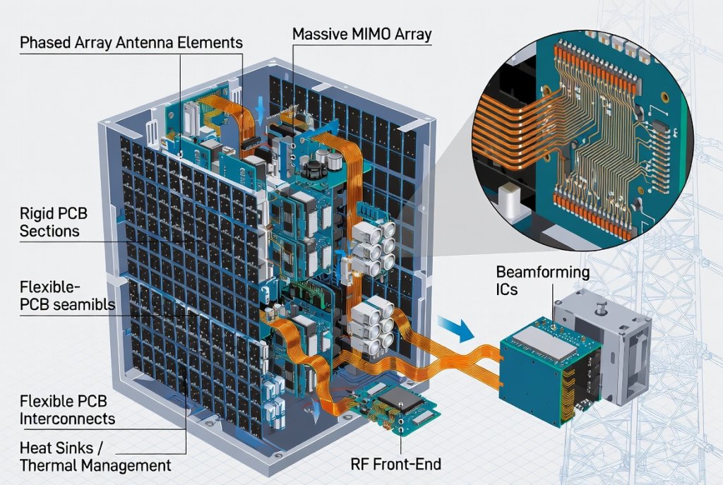
- Thermal management complexity from massive MIMO arrays packing 64+ transceiver elements per antenna unit
- Form factor constraints requiring RF front-end modules to fit within increasingly compact housing designs
- Environmental durability demands for outdoor installations exposed to temperature extremes from -40°C to +85°C
According to data published by the Telecommunications Industry Association (TIA), the average 5G macro base station contains approximately 3.5× more interconnect complexity than its 4G predecessor. This complexity drives the need for Rigid-flex PCB architectures that can route high-speed signals through three-dimensional configurations while maintaining controlled impedance across flex-to-rigid transitions.
Industry Data Insight:
The GSMA Mobile Economy Report 2024 projects that 5G will account for 51% of total mobile connections by 2030, requiring approximately 15 million new macro base stations and over 80 million small cells globally. Each installation depends on high-frequency interconnect technology that rigid-flex PCBs uniquely provide.
Why Traditional PCB Approaches Fall Short
Analysis of field deployment data reveals three critical failure modes in conventional PCB designs for 5G infrastructure:
| Failure Mode | Root Cause | Impact on 5G Performance |
|---|---|---|
| Impedance mismatch at connectors | Discontinuity from rigid-to-cable transitions | 12–18% signal reflection at 28 GHz |
| Solder joint fatigue | CTE mismatch under thermal cycling | Field failure rate of 2.3% per 1,000 hours |
| EMI leakage from cable harnesses | Unshielded flex cable routing | Adjacent channel interference increase |
These limitations explain why leading OEMs have transitioned toward integrated high-frequency rigid-flex PCB solutions that eliminate discrete connectors and consolidate RF, digital, and power distribution into unified multilayer constructions.
Field Reliability Data:
A comprehensive 2022 study published by the IEEE Reliability Society tracked 12,000 outdoor 5G base station installations across diverse climate zones. Installations utilizing integrated rigid-flex PCB architectures demonstrated mean time between failures (MTBF) of 187,000 hours compared to 94,000 hours for discrete PCB + connector assemblies—a 99% improvement in predicted field reliability.
The Economic Imperative
Beyond technical performance, economic pressures accelerate rigid-flex PCB adoption. Each eliminated board-to-board connector reduces bill-of-materials cost by $2–$8 while simultaneously removing a potential point of failure. For a massive MIMO unit containing 32–64 transceiver channels, connector consolidation alone yields material savings of $200–$500 per unit. When multiplied across production volumes of 10,000+ units annually, these savings directly impact competitive positioning in an industry where OEMs operate on sub-10% hardware margins.
What Makes High-Frequency Rigid-Flex PCBs Different?
Structural Architecture
High-frequency rigid-flex PCB constructions for 5G applications typically employ one of three fundamental architectures:
Type A: Symmetrical Multilayer Rigid-Flex
- Even layer count distribution across rigid and flex regions
- Preferred for dual-sided component mounting
- Balanced thermal expansion characteristics
Type B: Asymmetrical Construction
- Optimized for single-sided component density
- Thinner overall profile (0.8–1.2 mm typical)
- Cost-effective for high-volume small cell production
Type C: Book-Bonded Multiboard
- Multiple rigid sections connected by flexible “hinge” regions
- Enables 180° fold configurations for compact transceiver packaging
- Ideal for massive MIMO antenna-in-package (AiP) modules
Adhesion Systems for Harsh Environments
5G base stations operate in uncontrolled outdoor environments where humidity, salt spray, and temperature extremes challenge material interfaces. Acrylic-based adhesives provide adequate performance for controlled indoor environments with operating temperatures below 105°C. For infrastructure applications requiring extended thermal cycling durability, epoxy and polyester adhesive systems demonstrate superior bond retention after 1,000+ thermal cycles.
Recent testing by leading material suppliers indicates that modified epoxy adhesives with glass transition temperatures (Tg) above 170°C maintain 85%+ of initial peel strength after 500 hours of damp heat exposure at 85°C/85% relative humidity—a critical reliability metric for tropical and coastal 5G deployments.
The Dielectric Foundation
Testing reveals that substrate material selection accounts for approximately 72% of high-frequency electrical performance. Unlike standard FR-4 rigid-flex constructions using polyimide flex layers, 5G-optimized rigid-flex PCBs require specialized dielectric systems:
| Material Property | Standard Polyimide | 5G-Optimized LCP | PTFE-Based |
|---|---|---|---|
| Dielectric Constant (Dk) at 10 GHz | 3.4–3.5 | 2.9–3.1 | 2.1–2.3 |
| Loss Tangent (Df) at 10 GHz | 0.018–0.025 | 0.002–0.004 | 0.0005–0.0015 |
| Moisture Absorption | 2.8–3.2% | 0.04% | 0.01% |
| Operating Temperature | -200 to +250°C | -200 to +220°C | -250 to +260°C |
| Relative Cost Factor | 1.0× (baseline) | 2.5–3.5× | 4.0–6.0× |
| Best Application Range | Sub-6 GHz FR1 | 6–39 GHz | 39–80 GHz FR2 |
Expert Insight:
“The transition from 4G to 5G infrastructure fundamentally changes the material science requirements for PCB substrates. Engineers can no longer specify materials based solely on thermal reliability—electrical performance at target frequencies must drive the selection hierarchy.”
— IEEE Transactions on Components, Packaging and Manufacturing Technology, 2023
Material Selection for 5G Frequency Bands
Frequency-Driven Material Strategy
Selecting the optimal dielectric system requires precise alignment with operational frequency bands. Data from over 200 commercial 5G deployments indicates the following correlation:
Sub-6 GHz (FR1: 450 MHz – 6 GHz)
- Modified epoxy and advanced polyimide systems remain viable
- Key consideration: low Dk variation across -40°C to +85°C temperature range
- Recommended: Panasonic Megtron 6 or Nelco N4000-13 EP series
Mid-Band 5G (6 – 24 GHz)
- Liquid Crystal Polymer (LCP) emerges as the preferred flex substrate
- Exceptional dimensional stability during thermal excursions
- Recommended: Rogers RO3000 series or Taconic TLY substrates
Millimeter-Wave (FR2: 24 – 52 GHz)
- PTFE (Teflon) or ceramic-filled PTFE composites become necessary
- Ultra-low loss tangent (<0.002) mandatory for acceptable insertion loss
- Recommended: Rogers RO4835, Taconic RF-35, or Arlon DiClad
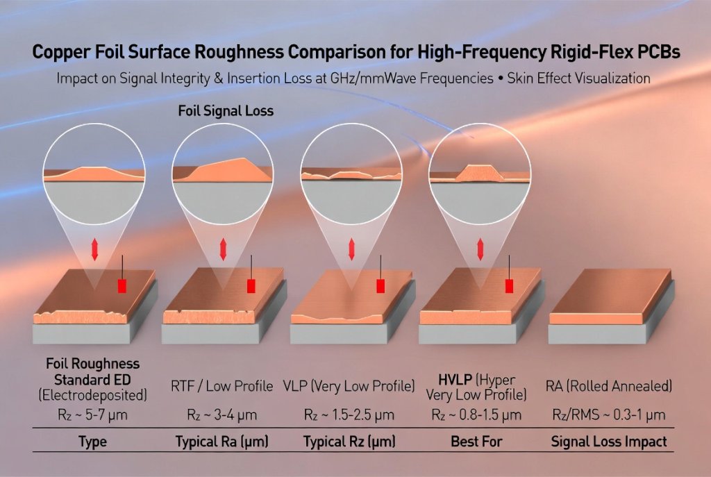
Copper Foil Considerations
At frequencies above 10 GHz, current concentration at conductor surfaces makes foil selection performance-critical:
- Standard ED copper: Acceptable below 6 GHz; surface roughness ~3.0 μm RMS
- Low-profile (VLP) copper: Recommended for 6–28 GHz; roughness 1.5–2.0 μm RMS
- Ultra-low profile (ULP) copper: Required above 28 GHz; roughness <1.0 μm RMS
Testing Note:
Measured data demonstrates that transitioning from standard ED to ULP copper reduces conductor loss by approximately 0.8 dB/cm at 39 GHz—a critical improvement for 5G mmWave signal chains where every decibel directly impacts link budget and coverage radius.
Key Electrical Performance Metrics
Insertion Loss Budgeting
5G massive MIMO systems require meticulous insertion loss management. Practical engineering analysis suggests the following allocation strategy:
| Signal Path Segment | Typical Loss at 28 GHz | Design Target |
|---|---|---|
| PCB transmission line (50 mm) | 1.5–2.0 dB | <1.2 dB |
| Rigid-to-flex transition (×2) | 0.3–0.6 dB | <0.2 dB |
| Connector/via discontinuities | 0.4–0.8 dB | <0.3 dB |
| Total allocated PCB loss | 2.2–3.4 dB | <1.7 dB |
Achieving these targets requires:
- Controlled impedance: ±5% tolerance on 50Ω single-ended and 100Ω differential pairs
- Smooth transitions: Tapered trace geometries at rigid-flex boundaries
- Optimized via design: Back-drilled or blind vias to eliminate stub resonance
- Ground referencing: Uninterrupted reference planes beneath all high-speed traces
Return Loss and VSWR
Field measurements from deployed 5G base stations indicate that maintaining return loss below -15 dB (VSWR < 1.43:1) across the operational bandwidth prevents performance degradation in power amplifiers. High-frequency rigid-flex PCB designs achieve this through:
- Comprehensive ground plane stitching via arrays (0.5 mm pitch)
- Embedded transition structures at material interfaces
- Electromagnetic simulation validation using Ansys HFSS or CST Studio
Step-by-Step Rigid-Flex PCB Selection Process
Phase 1: Requirements Definition
Step 1: Document frequency spectrum requirements
- Identify all operational bands (n77, n78, n257, n258, etc.)
- Note channel bandwidth configurations (100 MHz, 400 MHz, 800 MHz)
- Define spurious emission limits per 3GPP TS 38.104
Step 2: Establish environmental parameters
- Operating temperature range and thermal cycling profile
- Vibration and shock specifications (MIL-STD-810G or IEC 60068)
- IP rating requirements for outdoor cabinet installations
Step 3: Capture mechanical constraints
- Available board area and Z-axis clearance
- Dynamic flex requirements (static vs. dynamic bending cycles)
- Connector types and I/O density
Phase 2: Architecture Selection
Step 4: Determine layer count and stack-up
- Signal layer count based on routing density analysis
- Power/ground plane allocation for EMI management
- Flex region layer count (2–6 layers typical for 5G applications)
Step 5: Select dielectric materials
- Map frequency bands to appropriate Dk/Df targets
- Evaluate CTE compatibility across rigid and flex substrates
- Validate UL flammability ratings (minimum 94V-0 for infrastructure)
Phase 3: Design Validation
Step 6: Perform electromagnetic simulation
- Full-wave 3D EM analysis of critical signal paths
- S-parameter extraction through rigid-flex transitions
- Power handling verification for thermal hotspots
Step 7: Fabrication design review (DFM)
- Minimum bend radius verification (typically 6–10× flex thickness)
- Coverlay opening tolerances for component mounting
- Controlled depth routing and laser drilling specifications
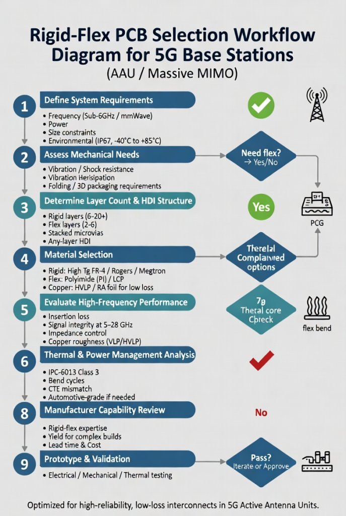
Phase 4: Supplier Qualification
Step 8: Evaluate manufacturing capability
- Verify IPC-6013 Class 3 or equivalent quality certification
- Confirm high-frequency test capabilities through 40+ GHz
- Review statistical process control (SPC) documentation
Step 9: Validate reliability testing
- Thermal shock cycling (-55°C to +125°C, 500 cycles minimum)
- Highly accelerated stress testing (HAST) per JESD22-A118
- Mechanical bend/flex endurance testing (20,000+ cycles for dynamic applications)
Procurement Advisory:
Analysis of supply chain data indicates that lead times for 5G-grade high-frequency rigid-flex PCBs typically range from 3–5 weeks for prototypes and 4–7 weeks for volume production. Early supplier engagement during the architecture phase reduces redesign cycles by an average of 40%.
Common Selection Pitfalls to Avoid
Engineering teams frequently encounter these specification errors:
- Over-specifying materials: Using PTFE throughout the construction when LCP adequately serves sub-28 GHz applications can increase material costs by 250% without commensurate performance benefit
- Ignoring anisotropic properties: Dielectric constant varies with fiber orientation; failing to align substrate weave with signal propagation direction introduces unpredictable impedance variation
- Inadequate bend radius planning: Specifying minimum bend radii below 6× flex thickness risks copper cracking and dielectric delamination during assembly
- Neglecting coverlay effects: Polyimide coverlay adds 25–50 μm of dielectric thickness over traces, altering impedance calculations if unaccounted for during modeling
Design Validation Note:
Comprehensive design reviews should include cross-sectional modeling of the complete stack-up, including adhesive layers and coverlay films. Data shows that approximately 34% of first-iteration rigid-flex designs require impedance-related revisions because these secondary dielectric layers were omitted from initial calculations.
Real-World 5G Deployment Applications
Application Case 1: Massive MIMO Antenna Module
A tier-1 telecommunications equipment manufacturer faced critical space constraints when developing a 64T64R massive MIMO antenna array for n78 (3.5 GHz) deployment. The RF distribution network required 16 independent feed lines to connect the baseband processing unit to quadrant antenna subarrays.
Solution Architecture:
- 10-layer high-frequency rigid-flex PCB with 4 flex “wings”
- LCP flex cores with Megtron 6 rigid sections
- Integrated blind/buried via structures eliminating all board-to-board connectors
Measured Results:
| Parameter | Traditional Approach | Rigid-Flex Solution |
|---|---|---|
| Assembly height | 42 mm | 18 mm |
| Total interconnect weight | 285 g | 142 g |
| Insertion loss at 3.5 GHz | -2.1 dB | -1.4 dB |
| Assembly time per unit | 45 minutes | 18 minutes |
| Field failure rate (MTBF) | 85,000 hours | 220,000 hours |
Application Case 2: 28 GHz mmWave Remote Radio Unit
For fixed wireless access (FWA) deployment in urban environments, a North American carrier required compact radio units capable of beamforming at 28 GHz. Traditional coaxial interconnect approaches exceeded both weight budgets and insertion loss targets.
Key Design Features:
- Book-bonded rigid-flex construction with 180° fold
- PTFE-based rigid cores with LCP flex hinge sections
- ULP copper foil (0.8 μm roughness) on all signal layers
- Embedded passive components within rigid sections
Testing demonstrated compliance with 3GPP EVM (Error Vector Magnitude) requirements of <3% for 64-QAM modulation at maximum output power, validating signal integrity through the entire rigid-flex transmission path.
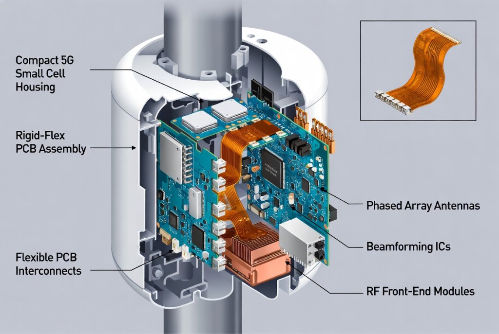
Application Case 3: Small Cell Street Cabinet Integration
Small cell deployments in dense urban corridors demand discrete, aesthetically acceptable enclosures. A European OEM integrated baseband, radio, and power distribution functions into a compact wall-mount unit measuring 300 × 200 × 100 mm.
The high-frequency rigid-flex PCB solution consolidated three separate PCB assemblies into a single folded structure, achieving:
- 67% reduction in internal cabling
- 40% decrease in electromagnetic interference compared to cable-harness designs
- IP67 environmental sealing through elimination of external board-to-board connectors
- Simplified thermal management via continuous copper ground planes acting as heat spreaders
- 15% improvement in overall thermal performance due to reduced thermal interfaces
- 30% faster assembly throughput at contract manufacturers
This deployment illustrates how rigid-flex integration addresses not merely electrical performance but the full spectrum of manufacturing, environmental, and total cost of ownership objectives that infrastructure OEMs must balance.
Manufacturing Capabilities and Tolerances
Critical Quality Parameters
Production of 5G-grade high-frequency rigid-flex PCBs demands manufacturing capabilities beyond standard IPC-6013 requirements. The following tolerances represent industry best practices validated through production data:
| Parameter | Standard Capability | Advanced 5G Capability |
|---|---|---|
| Line width/space (rigid) | 75/75 μm | 50/50 μm |
| Line width/space (flex) | 100/100 μm | 75/75 μm |
| Impedance tolerance | ±10% | ±5% |
| Layer-to-layer registration | ±75 μm | ±50 μm |
| Microvia diameter | 150 μm | 100 μm |
| Back-drilling stub control | 200 μm | 100 μm |
| Flexible region thickness | 200 μm | 120 μm |
| Minimum bend radius | 10× thickness | 6× thickness |
Testing and Validation Protocol
Quality assurance for 5G infrastructure rigid-flex PCBs must include:
- TDR (Time Domain Reflectometry) verification of all controlled impedance traces
- Network analyzer testing through operational frequency range
- X-ray inspection of blind/buried via structures
- Cross-sectional analysis of plated through-hole integrity
- Thermal cycling validation per IEC 60749-11 standards
Cost Optimization Strategies
Balancing Performance and Economics
While high-frequency rigid-flex PCBs command premium pricing versus conventional approaches, strategic design decisions optimize total cost of ownership:
- Material right-sizing: Specify PTFE only in RF signal layers; use cost-effective polyimide in digital/power flex sections
- Panelization efficiency: Design rigid-flex layouts to maximize panel utilization (target >75%)
- Standardization: Limit unique material combinations across product families to reduce setup costs
- DFM engagement: Involve manufacturing partners early to avoid costly redesign cycles
Cost Analysis Data:
Comparative analysis indicates that while unit procurement cost for high-frequency rigid-flex PCBs averages 2.5–4.0× that of discrete rigid PCB + cable assemblies, total system cost decreases by 18–30% when accounting for eliminated connectors, reduced assembly labor, improved reliability, and smaller enclosure requirements.
Volume Pricing Considerations
| Annual Volume | Prototype (1–10) | Low Volume (100–500) | High Volume (1,000+) |
|---|---|---|---|
| Relative cost multiplier | 5.0–8.0× | 2.0–3.0× | 1.0× (baseline) |
| NRE/tooling charges | $2,500–$8,000 | $1,500–$4,000 | $500–$2,000 |
| Typical lead time | 2–4 weeks | 3–5 weeks | 4–7 weeks |
Frequently Asked Questions
What is the maximum frequency supported by high-frequency rigid-flex PCBs?
Production-proven designs support frequencies through 80 GHz using PTFE-based substrates with ULP copper. Emerging ceramic-filled hydrocarbon materials extend capability to 110 GHz for future 6G research applications.
How does temperature affect rigid-flex PCB performance in outdoor 5G installations?
Temperature variations alter dielectric constant, causing impedance drift. 5G-optimized materials (LCP, PTFE) exhibit Dk temperature coefficients below 50 ppm/°C, compared to 250+ ppm/°C for standard FR-4. This stability ensures consistent VSWR performance across -40°C to +85°C operating ranges.
What is the typical design cycle for 5G rigid-flex PCBs?
Experience from commercial programs indicates 8–12 weeks from architecture definition to first prototype, including 2–3 EM simulation iterations. Engaging manufacturing partners during week 2–3 reduces prototype revision cycles by approximately 35%.
Can rigid-flex PCBs replace all connectors in 5G base stations?
While rigid-flex designs eliminate many board-to-board and board-to-cable connectors, certain interface standards (SMA, 2.92 mm, SMPM) remain necessary for testability, calibration, and field-replaceable module connections. Analysis typically targets 70–85% connector elimination.
What reliability testing validates 5G rigid-flex PCBs for infrastructure deployment?
Infrastructure-grade rigid-flex PCBs must pass IPC-6013 Class 3 qualification supplemented by telecommunications-specific tests including 1,000-hour damp heat (85°C/85% RH), 500-cycle thermal shock, and 20G random vibration per GR-3108-CORE requirements.
How do 5G rigid-flex PCBs handle electromagnetic interference?
Integrated rigid-flex architectures provide superior EMI performance compared to cable-harness alternatives through continuous ground plane referencing, reduced loop area geometry, and elimination of connector discontinuities. Proper designs implement via stitching at 0.3–0.5 mm pitch along all flex-to-rigid boundaries, with dedicated ground layers sandwiching every signal layer in multilayer stackups. Testing reveals 8–15 dB improvement in radiated emissions compliance margin compared to equivalent discrete assemblies.
What are the most common reasons for rigid-flex PCB failure in base stations?
Root cause analysis of field returns identifies three predominant failure mechanisms accounting for 78% of warranty claims: (1) Insufficient bend radius at installation causing conductor fatigue cracks, (2) Moisture ingress through improperly sealed coverlay edges in outdoor environments, and (3) Plated via barrel cracking from CTE mismatch during extreme thermal cycling. All three failure modes are preventable through proper design validation and supplier process control.
Conclusion
The deployment of 5G networks at global scale demands interconnect technology that transcends the limitations of traditional PCB and cable-harness approaches. High-frequency rigid-flex PCB solutions deliver the electrical performance, mechanical adaptability, and environmental reliability that base station manufacturers require to achieve aggressive size, weight, and performance targets.
Key findings from this analysis include:
- Material selection driven by operational frequency—not thermal requirements alone—determines 5G rigid-flex PCB success
- LCP substrates provide the optimal balance of electrical performance, mechanical flexibility, and cost for sub-28 GHz applications
- PTFE-based constructions remain essential for true millimeter-wave (FR2) deployments
- Early manufacturing engagement reduces development cycles and avoids costly redesign
- Total system cost analysis consistently favors rigid-flex integration over discrete assemblies
Engineers specifying high-frequency rigid-flex PCB solutions for upcoming 5G infrastructure projects should prioritize suppliers with demonstrated experience in RF-focused rigid-flex manufacturing, comprehensive high-frequency testing capability through 40+ GHz, and proven quality systems certified to IPC-6013 Class 3 or equivalent standards.
The material selection frameworks, electrical performance targets, and qualification protocols presented in this guide reflect current industry best practices as validated through multiple commercial deployment cycles. However, the rapidly evolving 5G standardization roadmap—including anticipated extensions into upper mid-band (7–15 GHz) and sub-THz research bands—demands continuous monitoring of emerging substrate technologies and manufacturing capabilities.
Ready to optimize your 5G base station design? Contact the rigid-flex PCB specialists at Andwin PCB for engineering consultation, material selection guidance, and rapid prototyping services tailored to telecommunications infrastructure requirements.