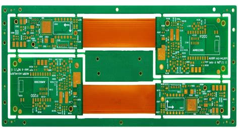
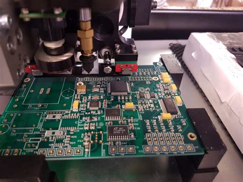
Hot air leveling process exposed copper analysis
Hot air leveling involves immersing the printed circuit board in molten solder (63SN/37PB) and then blowing hot air over the surface of the printed circuit board and the excess solder in the metalized hole to obtain a smooth, uniform, and bright solder coating. Cladding. After the hot air leveling, the surface of the tin-alloy coating on the surface of the printed circuit board should be bright and uniform, with good solderability, no nodules and no semi-wetting, and the coating is completely free of exposed copper. After the hot air leveling, the exposed copper on the surface of the pad and the metalized hole is an important defect in the inspection of the finished product. It is one of the common causes of hot air re-leveling and rework. There are many reasons for this problem, and the following are common.
1. The pre-processing is not enough and the roughening is bad.
The quality of the hot air leveling process is affected by the quality of the hot air pre-treatment process of the PCB. The process must completely remove the oil, impurities, and oxide layers on the pad, and provide a fresh solderable copper surface for the dipping tin.
The pretreatment process that is used more often now is mechanical spraying, firstly sulfuric acid-hydrogen peroxide microetching, acid etching after microetching, then water showering, hot air drying, flux injection, and immediate hot air leveling.
The phenomenon of exposed copper caused by poor pre-treatment is simultaneously occurring in a large number of batches regardless of the batch type. The copper dew point is often distributed over the entire board surface, and is more severe at the edges. Using a magnifying glass to observe the preprocessed circuit board will reveal significant residual oxidation spots and smudges on the pads.
A similar situation should occur for the chemical analysis of the microetch solution, check the second acid solution, adjust the concentration of the solution, replace the solution due to excessively long time contamination, and check whether the spray system is smooth. Appropriately prolonging the treatment time can also improve the treatment effect, but it is necessary to pay attention to the phenomenon of over-corrosion. The reworked circuit board is treated with a hot air leveling post-treatment line in a 5% hydrochloric acid solution to remove surface oxides.
2. The surface of the pad is dirty, and residual solder resist contaminates the pad.
At present, most manufacturers use full-screen screen printing liquid photosensitive resist ink, and then remove excess solder resist by exposure, development, get the time of the solder mask. In this process, the pre-bake process is not well controlled, and excessively high temperatures for too long can cause difficulties in development. Whether there are defects in the solder resist film, the composition and temperature of the developer is correct, the speed at the time of development is the correctness of the development point, whether the nozzle is blocked and the pressure of the nozzle is normal, and whether the water wash is good, any situation will give the pad Leave a remnant.
For example, the exposed copper formed due to the film is generally more regular and all at the same point. In this case, using a magnifying glass, traces of solder mask residues can be found at the exposed copper. In general, the PCB design should establish a post before the curing process to check the interior of the pattern and the metallization hole to ensure that the printed circuit board is sent to the next process. The pad and metallization holes clean the solderless ink residue.
3 flux activity is not enough
The function of the flux is to improve the wettability of the copper surface, protect the laminate surface from overheating, and provide protection for the solder coating. If the activity of the flux is not enough, the wettability of the copper surface is not good, and the solder cannot completely cover the pad. The copper exposure phenomenon is similar to the poor pre-treatment, and prolonging the pre-treatment time can reduce the copper exposure phenomenon. Current fluxes are almost all acidic fluxes and contain acidic additives. For example, excessive acidity can cause severe copper seizures. This can lead to high levels of copper in the solder and cause rough tin and tin; when the acidity is too low, the activity is weak and can lead to dew. copper. If the content of copper in the lead-tin bath is large, remove copper promptly. The process technicians choose a reliable and reliable flux for hot air leveling. The excellent flux is the guarantee of the leveling of the hot air.