
Skip to content
Andwin Circuits
  • Home
  • ProductsExpand
    • HDI multilayer PCB
    • Rigid Flex PCB
    • Flex pcb
    • Special PCBExpand
      • High Frequency PCBExpand
        • Rogers RO4350B PCB
        • Rogers RO4003 pcb
        • Rogers RO3003 PCB
        • Rogers 5880 PCB
        • DICLAD 527 PCB
        • Taconic TLX series
        • Taconic TLX-8 RF PCB
        • Taconic TLX-9 RF PCB
      • High speed pcbExpand
        • Megtron 6 High Speed PCB
        • TU-872 SLK Sp High Speed
      • High TG PCBExpand
        • SHENGYI SH260 PCB
        • ISOLA 370HR PCB
        • ISOLA IS410 PCB
        • ISOLA IS420 PCB
      • Heavy copper PCB
      • Copper coin pcb
      • Copper inlay PCB
    • Metal Core PCBExpand
      • Copper core pcb
      • Aluminum PCB
      • 2 Layers Aluminum PCB
      • Direct thermal MCPCB
      • 2 Layers Direct Thermal
    • Ceramic PCBExpand
      • DPC ceramic PCB
      • DBC ceramic PCB
      • Thick film Ceramic PCB
      • Al2O3 Alumina PCB
      • AIN ALN ceramic PCB
      • IGBT Ceramic PCB
  • ServiceExpand
    • PCB Assembly
    • Quick turn PCB assembly
    • PCBA conformal coating
  • IndustryExpand
    • Telecommunication
    • IoT and Wireless
    • Industrial Control
    • Thermal management
    • Power and Energy
    • IC test board
    • Automative
    • Medical
  • CapabilityExpand
    • Rigid PCB
    • Rigid flex PCB
    • Metal core PCB
    • PCB Assembly
  • TechnologyExpand
    • Blogs
    • Via in pad
    • PCB E-test
    • PCB stack up
    • MCPCB panelization
    • Controlled impedance PCB
  • AboutExpand
    • About us
    • Certification
    • Factory Tour
  • Contact
Andwin Circuits
Home / Blogs / How to Deal with Broken Traces in PCB Design: Causes, Prevention, and Solutions

How to Deal with Broken Traces in PCB Design: Causes, Prevention, and Solutions

ByGrace June 4, 2025March 31, 2026

Introduction

Printed Circuit Board (PCB) design is a complex process that requires precision and attention to detail. One common issue that designers encounter is broken traces (or “cut traces”), also known as “dead traces” or “disconnected traces.” These occur when a conductive pathway on the PCB is unintentionally interrupted, leading to open circuits and malfunctioning boards.

This article explores the causes of broken traces, methods to prevent them, and effective solutions to fix them during the design and manufacturing phases.

1. Causes of Broken Traces in PCB Design

Understanding why traces break helps in preventing and resolving the issue efficiently. Common causes include:

1.1. Manufacturing Defects

  • Insufficient Copper Etching: Over-etching can thin out traces, making them prone to breaking.
  • Drilling Errors: Misaligned or excessive drilling can sever traces.
  • Improper Lamination: Weak bonding between layers may cause trace separation.

1.2. Design Errors

  • Inadequate Trace Width: Thin traces are more susceptible to breaks during handling or thermal stress.
  • Sharp Angles: 90-degree bends increase stress concentration, leading to cracks.
  • Insufficient Clearance: Traces too close to board edges or drill holes may get cut during fabrication.

1.3. Mechanical Stress

  • Flexing or Bending: PCBs in flexible or high-vibration environments may develop fractures.
  • Improper Handling: Rough assembly processes can damage traces.

1.4. Environmental Factors

  • Thermal Cycling: Repeated heating and cooling weaken traces over time.
  • Corrosion: Exposure to moisture or chemicals can degrade copper traces.
Contact us for PCB quote now |

2. Prevention Strategies

Preventing broken traces is more efficient than repairing them. Key strategies include:

2.1. Optimizing Trace Design

  • Use Appropriate Trace Width: Follow IPC-2221 standards for current-carrying capacity.
  • Avoid Sharp Corners: Use 45-degree angles or curved traces to reduce stress.
  • Maintain Proper Spacing: Keep traces away from board edges and drill holes.

2.2. Design Rule Checks (DRC)

  • Run DRC in CAD Tools: Software like Altium Designer, KiCad, or Eagle can detect potential breaks.
  • Verify Manufacturing Constraints: Ensure trace widths and spacings match the PCB fab house’s capabilities.

2.3. Strengthening Critical Traces

  • Use Teardrops: Adding teardrops at via-to-trace junctions improves mechanical strength.
  • Add Redundant Paths: For high-reliability designs, duplicate critical traces.

2.4. Selecting the Right Manufacturer

  • Choose Reputable PCB Fab Houses: Experienced manufacturers reduce defects.
  • Specify Copper Weight: Thicker copper (e.g., 2 oz instead of 1 oz) improves durability.

3. How to Fix Broken Traces

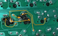
If a PCB already has broken traces, here are repair methods:

3.1. Manual Repair (For Prototypes)

  • Method 1: Jumper Wires
  • Identify the broken trace.
  • Use a thin enamel wire to bridge the gap.
  • Solder and secure with epoxy if needed.
  • Method 2: Conductive Pen or Paint
  • Apply conductive silver ink to reconnect the trace.
  • Cure as per manufacturer instructions.

3.2. PCB Rework (For Small Batches)

  • Scrape and Solder:
  • Gently scrape off solder mask over the broken trace.
  • Apply flux and solder to reconnect.
  • Copper Foil Patch:
  • Cut a small piece of copper tape.
  • Solder it over the broken section.

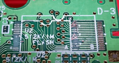
3.3. Advanced Repair (For High-Density Boards)

  • Microsoldering: Requires precision tools for fine-pitch components.
  • Laser Repair: Some professional services use laser welding for trace repairs.

3.4. Preventing Further Damage

  • Conformal Coating: Protects repaired traces from environmental damage.
  • Strain Relief: Add mechanical support to prevent flexing.
Contact us for PCB quote now |

4. Testing and Validation

After repair, verify functionality:

  • Continuity Testing: Use a multimeter to check trace connectivity.
  • Visual Inspection: Magnifying tools help spot weak joints.
  • Functional Testing: Power up the board and test signal integrity.

5. Conclusion

Broken traces in PCB design can lead to costly failures, but proper design practices, thorough DRC checks, and careful manufacturing selection can minimize risks. If breaks occur, manual repairs, conductive adhesives, or professional rework can restore functionality.

By understanding the root causes, applying preventive measures, and mastering repair techniques, PCB designers and engineers can ensure robust and reliable circuit boards.

Contact us for PCB quote now |
Post Tags: #aluminum clad pcb#aluminum core pcb#aluminum pcb#assemble pcb#broken trace in pcb#pcb design

Post navigation

Previous Previous
Preparation Processes Before PCB Copper Electroplating
NextContinue
How to Quickly Analyze PCB Design Risk Issues

Search

Search

Products

  • HDI Multilayer PCB
  • Rigid Flex PCB
  • Flex pcb
  • High Frequency PCB
  • High speed pcb
  • Heavy copper PCB
  • Metal Core PCB
  • Ceramic PCB

Address

Andwin Circuits Co.,Limited
Email: sales@andwinpcb.com
Tel: +86 755 2832 9394
Fax:+86 755 2992  6717
ADD:1-2F-1217,HouDeQun Industrial park,
NanTing RD NO.56,ShaJing,BaoAn,Shenzhen 518104,GuangDong,China

Products

  • HDI Multilayer PCB
  • Rigid Flex PCB
  • Flex pcb
  • High Frequency PCB
  • High speed pcb
  • Heavy copper PCB
  • Metal Core PCB
  • Ceramic PCB

Technology

  • Blogs
  • Via in pad
  • PCB E-test
  • PCB stack up
  • Metal core PCB panelization
  • Controlled impedance PCB

CERTIFICATION

Certification >>


Copyright© 2003 - 2026 Andwin | All Rights Reserved | Powered by Andwin

Scroll to top
  • Home
  • Products
    • HDI multilayer PCB
    • Rigid Flex PCB
    • Flex pcb
    • Special PCB
      • High Frequency PCB
        • Rogers RO4350B PCB
        • Rogers RO4003 pcb
        • Rogers RO3003 PCB
        • Rogers 5880 PCB
        • DICLAD 527 PCB
        • Taconic TLX series
        • Taconic TLX-8 RF PCB
        • Taconic TLX-9 RF PCB
      • High speed pcb
        • Megtron 6 High Speed PCB
        • TU-872 SLK Sp High Speed
      • High TG PCB
        • SHENGYI SH260 PCB
        • ISOLA 370HR PCB
        • ISOLA IS410 PCB
        • ISOLA IS420 PCB
      • Heavy copper PCB
      • Copper coin pcb
      • Copper inlay PCB
    • Metal Core PCB
      • Copper core pcb
      • Aluminum PCB
      • 2 Layers Aluminum PCB
      • Direct thermal MCPCB
      • 2 Layers Direct Thermal
    • Ceramic PCB
      • DPC ceramic PCB
      • DBC ceramic PCB
      • Thick film Ceramic PCB
      • Al2O3 Alumina PCB
      • AIN ALN ceramic PCB
      • IGBT Ceramic PCB
  • Service
    • PCB Assembly
    • Quick turn PCB assembly
    • PCBA conformal coating
  • Industry
    • Telecommunication
    • IoT and Wireless
    • Industrial Control
    • Thermal management
    • Power and Energy
    • IC test board
    • Automative
    • Medical
  • Capability
    • Rigid PCB
    • Rigid flex PCB
    • Metal core PCB
    • PCB Assembly
  • Technology
    • Blogs
    • Via in pad
    • PCB E-test
    • PCB stack up
    • MCPCB panelization
    • Controlled impedance PCB
  • About
    • About us
    • Certification
    • Factory Tour
  • Contact
Search