
How to Ensure PCB Design Files Meet SMT Assembly Requirements
Introduction
Surface Mount Technology (SMT) has become the dominant method for PCB assembly in modern electronics manufacturing. To ensure smooth and cost-effective production, PCB designers must create design files that fully comply with SMT manufacturing requirements. This comprehensive guide outlines critical considerations and best practices to prepare your PCB design files for successful SMT assembly.
1. Understanding SMT Process Requirements
1.1 SMT Assembly Workflow
Before designing for SMT, understand the complete assembly process:
- Solder paste application (stencil printing)
- Component placement (pick-and-place machines)
- Reflow soldering
- Inspection (AOI and/or AXI)
- Testing
1.2 Manufacturer Capabilities
Always consult with your manufacturer about:
- Minimum component sizes they can handle
- Placement accuracy tolerances
- Panelization preferences
- Preferred file formats and deliverables
2. PCB Design File Preparation
2.1 Required Files for SMT Assembly
Provide these complete and accurate files:
- Gerber files (RS-274X format preferred)
- Drill files (Excellon format)
- Centroid file (pick-and-place file)
- Bill of Materials (BOM)
- Assembly drawings
- Schematic diagram
2.2 Layer Stackup Considerations
- Clearly define layer stackup including copper weights
- Specify solder mask and silkscreen colors
- Include impedance control requirements if needed
- Provide material specifications (FR-4, high-Tg, etc.)
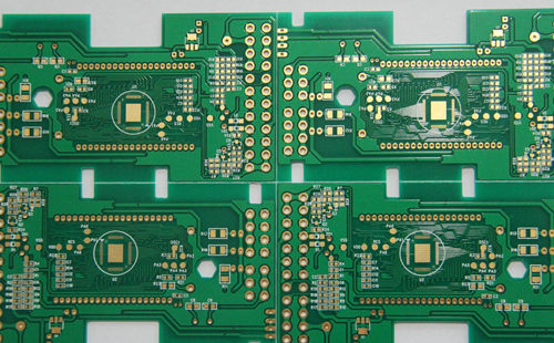
3. Component Placement Guidelines
3.1 Component Spacing Requirements
- Maintain adequate clearance between components (typically 0.5mm minimum)
- Consider reflow shadow effects for taller components
- Ensure sufficient space for rework and inspection
3.2 Orientation and Placement
- Standardize component orientation (0° or 90°)
- Avoid placing small components near large ones
- Consider nozzle size requirements for pick-and-place machines
3.3 Polarized Components
- Clearly mark polarity on silkscreen
- Consistent orientation for easier inspection
- Verify footprint matches component datasheet
4. Land Pattern Design
4.1 IPC-Compliant Footprints
- Follow IPC-7351 standards for land patterns
- Ensure proper pad sizes for reliable solder joints
- Include appropriate solder mask openings
4.2 Special Considerations
- Fine-pitch components (QFN, BGA, etc.)
- Thermal pads for heat dissipation
- Mechanical stress points (connectors, switches)
5. Solder Mask and Silkscreen
5.1 Solder Mask Requirements
- Minimum clearance around pads (typically 0.05-0.1mm)
- Avoid solder mask between fine-pitch pads
- Specify solder mask expansion values
5.2 Silkscreen Best Practices
- Clear component designators and polarity marks
- Avoid silkscreen over pads or vias
- Minimum line width (typically 0.15mm)
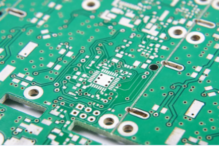
6. Stencil Design Considerations
6.1 Aperture Design
- Proper aperture size relative to pad
- Special shapes for challenging components
- Area ratio calculations for proper paste release
6.2 Framing and Fiducials
- Include global and local fiducials
- Standard stencil frame dimensions
- Clear stencil identification markings
7. Panelization Design
7.1 Breakaway Methods
- V-scoring parameters (depth, angle)
- Tab routing (number and size of tabs)
- Perforations for specific materials
7.2 Panel Features
- Tooling holes and alignment marks
- Test coupons for process control
- Balanced copper distribution
8. Design for Manufacturing (DFM) Checks
8.1 Common DFM Issues
- Insufficient solder mask web
- Acid traps in copper pours
- Drill-to-copper clearance violations
- Silkscreen over pads
8.2 DFM Validation Tools
- Use automated DFM checking software
- Manufacturer’s DFM guidelines
- Third-party design review services
9. Thermal Management
9.1 Reflow Considerations
- Balanced component distribution
- Thermal mass equalization
- Sensitive component placement
9.2 Heat Dissipation
- Thermal via patterns
- Copper balancing
- High-temperature materials
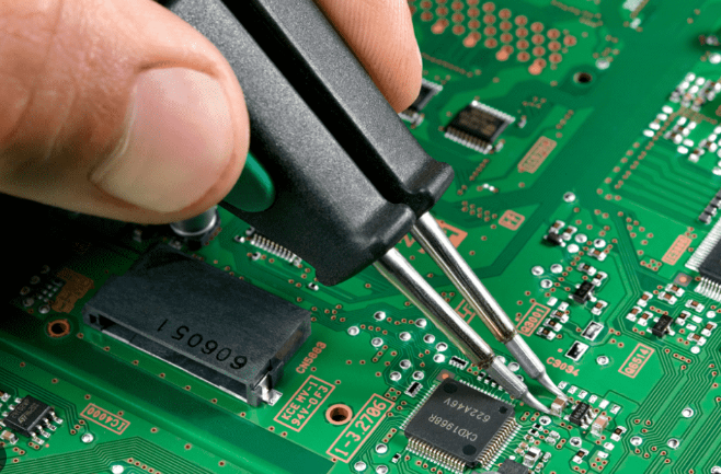
10. Testing and Inspection Requirements
10.1 Test Point Placement
- Adequate spacing for probe access
- Standardized test point sizes
- ICT and flying probe considerations
10.2 AOI Requirements
- Sufficient contrast for vision systems
- Avoid reflective surfaces
- Component height variations
11. Documentation Requirements
11.1 Assembly Drawings
- Layer stackup diagram
- Critical dimensions
- Special instructions
11.2 BOM Preparation
- Complete manufacturer part numbers
- Alternatives and substitutions
- Reference designators matching layout
12. Communication with Manufacturers
12.1 Early Engagement
- Involve manufacturers during design phase
- Clarify special requirements
- Understand their capabilities
12.2 Change Management
- Clear revision control
- Engineering change orders (ECOs)
- Prototype feedback incorporation
Conclusion
Ensuring PCB design files meet SMT assembly requirements requires attention to numerous technical details and close collaboration with manufacturing partners. By following these guidelines, designers can significantly improve first-pass yield, reduce manufacturing costs, and accelerate time-to-market. Always remember that the most successful designs balance electrical performance with manufacturability, creating products that are both functional and economical to produce in volume.