How to Generate PCB in Proteus: A Step-by-Step Guide
Introduction
Proteus is a powerful software suite widely used for electronic design automation (EDA). It offers schematic capture, simulation, and PCB (Printed Circuit Board) layout design capabilities. One of its most useful features is the ability to convert a schematic diagram into a PCB design seamlessly. This article provides a comprehensive guide on how to generate a PCB in Proteus, covering schematic design, component placement, routing, and final output generation.
Step 1: Designing the Schematic
Before generating a PCB, you must first create a schematic diagram of your circuit. Follow these steps:
1.1 Launch Proteus and Create a New Project
- Open Proteus ISIS (the schematic capture module).
- Go to File → New Project.
- Enter a project name and select a save location.
- Choose “Create a schematic from the selected template” (default settings are usually fine).
- Click Next, then Finish.
1.2 Add Components to the Schematic
- Click the Component Mode button (usually labeled “P”).
- Search for components (e.g., resistors, capacitors, ICs) in the Pick Devices window.
- Select components and place them on the schematic workspace.
1.3 Wire the Components
- Use the Wire Tool to connect components as per your circuit design.
- Ensure all connections are correct to avoid errors in PCB generation.
1.4 Assign PCB Packages
Each component in Proteus must have an associated PCB footprint (a physical representation on the PCB).
- Right-click a component and select “Edit Properties”.
- In the PCB Package field, assign the correct footprint (e.g., RES40 for a through-hole resistor).
- Repeat for all components.
Step 2: Switching to PCB Layout
Once the schematic is complete, you can proceed to PCB design.
2.1 Open the PCB Layout Module
- In Proteus ISIS, go to Tools → Netlist to ARES (or press Ctrl + N).
- This opens Proteus ARES, the PCB design module.
2.2 Verify Components and Netlist
- ARES will load all components from the schematic.
- Check for errors (e.g., missing footprints). If any component lacks a footprint, return to ISIS and assign one.
Step 3: PCB Layout Design
Now, you can arrange components and route traces.
3.1 Component Placement
- Drag and place components in logical positions (e.g., connectors near edges, ICs centrally).
- Use Rotation (Ctrl + R) to adjust component orientation.
- Ensure components do not overlap.
3.2 Define Board Outline
- Select the 2D Graphics Box Mode (usually in the toolbar).
- Draw the PCB boundary (e.g., a rectangle matching your desired PCB size).
3.3 Autorouting vs. Manual Routing
Proteus supports both manual and automatic routing.
Option 1: Autorouting
- Click Tools → Auto Router.
- Configure routing settings (e.g., track width, via size).
- Click Begin Routing and let Proteus generate traces automatically.
Option 2: Manual Routing
- Select the Track Mode tool.
- Click on component pads and draw traces manually.
- Use different layers (e.g., Top Copper, Bottom Copper) for complex designs.
3.4 Design Rule Check (DRC)
Before finalizing, run a DRC to detect errors:
- Go to Tools → Design Rule Check.
- Fix any spacing, clearance, or unconnected net errors.
Step 4: Generating Output Files
Once the PCB layout is complete, generate manufacturing files.
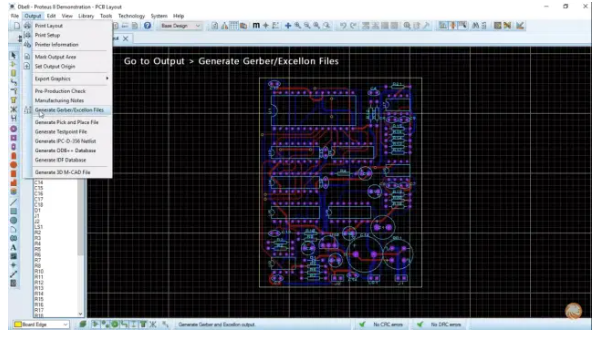
4.1 Gerber Files (For PCB Fabrication)
- Go to Output → Gerber/Excellon Output.
- Select layers (e.g., Top Copper, Bottom Copper, Silkscreen).
- Click OK to generate Gerber files (sent to PCB manufacturers).
4.2 Drill Files (For Hole Drilling)
- In the same Gerber/Excellon Output window, ensure Excellon Drill File is selected.
- Generate the drill file for PCB drilling machines.
4.3 3D Visualization
Proteus allows 3D PCB preview:
- Go to Output → 3D Visualization.
- Inspect the PCB in 3D to check component placement.
4.4 Bill of Materials (BOM)
Generate a BOM for component procurement:
- In ISIS, go to Tools → Bill of Materials.
- Export as CSV or PDF.

Conclusion
Proteus provides a streamlined workflow from schematic design to PCB generation. By following these steps—designing the schematic, assigning footprints, arranging components, routing traces, and generating manufacturing files—you can efficiently create a professional PCB layout. Whether using autorouting for simplicity or manual routing for precision, Proteus offers the tools needed for successful PCB design.
For beginners, practicing with simple circuits before tackling complex designs is recommended. With experience, you can leverage Proteus’ advanced features (e.g., multilayer PCBs, high-speed routing) for more sophisticated projects.
Would you like additional details on any specific step? Let me know how I can assist further!