How to Properly Operate PCB Panelization: A Comprehensive Guide
Introduction
Printed Circuit Board (PCB) panelization is a crucial step in the PCB manufacturing process that involves arranging multiple PCB designs onto a single panel for efficient production. Proper panelization ensures cost-effectiveness, improves assembly efficiency, and enhances the overall quality of the final product. However, incorrect panelization can lead to manufacturing defects, increased costs, and assembly difficulties.
This article provides a detailed guide on how to correctly perform PCB panelization, covering key considerations such as panel design, tooling requirements, breakaway methods, and best practices for optimal results.
1. Understanding PCB Panelization
PCB panelization is the process of grouping multiple PCBs onto a single larger board (panel) to streamline manufacturing, assembly, and testing. This technique is widely used in mass production to reduce material waste, improve handling efficiency, and lower production costs.
Types of PCB Panelization
There are two primary methods of PCB panelization:
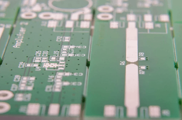
- Tab Routing (V-Groove Panelization) – Uses V-shaped grooves between PCBs, allowing easy separation after assembly.
- Breakaway Tabs (Mouse Bites) – Small perforated tabs hold PCBs together, which are later broken apart.
Each method has its advantages and should be chosen based on the PCB design and assembly requirements.
2. Key Considerations for PCB Panelization
A. Panel Size and Standardization
Manufacturers often use standard panel sizes (e.g., 18″ x 24″, 21″ x 24″) to optimize fabrication efficiency. Designers should:
- Confirm the manufacturer’s preferred panel dimensions.
- Avoid exceeding maximum panel size limits.
- Ensure sufficient clearance between PCBs (typically 2-5mm).
B. Spacing and Clearance
Proper spacing between PCBs prevents damage during depaneling. Key guidelines include:
- For V-Groove Panelization: Maintain at least 1/3 of the PCB thickness in remaining material for structural integrity.
- For Breakaway Tabs: Use 0.5mm to 1mm perforations (mouse bites) with 0.3mm to 0.5mm tab widths.
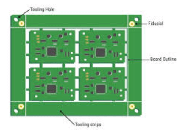
C. Fiducial Marks and Tooling Holes
Fiducial marks (alignment markers) and tooling holes ensure precise assembly. Best practices include:
- Place at least three fiducial marks per panel (preferably in a triangular pattern).
- Include tooling holes (typically 3mm diameter) for secure handling during assembly.
D. Copper Balancing
Uneven copper distribution can cause warping during reflow soldering. To prevent this:
- Add dummy copper areas in sparse regions.
- Ensure symmetrical copper layers in multilayer PCBs.
E. Depaneling Method Selection
The chosen depaneling method affects panel design:
- V-Scoring: Best for straight-line separation; unsuitable for complex shapes.
- Breakaway Tabs: Ideal for irregular PCB shapes but may require manual breaking.
- Laser Cutting: High precision but more expensive.
3. Step-by-Step PCB Panelization Process
Step 1: Design PCB Layout
- Use CAD software (e.g., Altium, KiCad, Eagle) to arrange multiple PCBs on a panel.
- Maintain consistent spacing and orientation.
Step 2: Add Breakaway Tabs or V-Grooves
- For tab routing, place small tabs (0.5-1mm wide) with perforations.
- For V-grooves, ensure a 30°-45° cutting angle with sufficient remaining material.
Step 3: Include Fiducials and Tooling Holes
- Place fiducials near panel corners and tooling holes for alignment.
Step 4: Verify Design Rules
- Check for minimum spacing, copper balance, and depaneling feasibility.
- Run a Design for Manufacturability (DFM) check.
Step 5: Export Gerber Files and Panel Drawings
- Provide manufacturers with Gerber files, drill files, and assembly drawings.
4. Common PCB Panelization Mistakes to Avoid
Mistake 1: Insufficient Spacing Between PCBs
- Leads to cracking during depaneling.
- Solution: Follow manufacturer-recommended clearances.
Mistake 2: Incorrect Tab Placement
- Weak tabs cause premature breakage.
- Solution: Use at least 3-4 tabs per side for stability.
Mistake 3: Ignoring Copper Balance
- Causes warping during reflow soldering.
- Solution: Distribute copper evenly or add thieving pads.
Mistake 4: Overlooking Fiducial Marks
- Misalignment during assembly.
- Solution: Always include fiducials in panel design.
5. Best Practices for Effective PCB Panelization
- Consult the Manufacturer Early – Confirm panel size and depaneling capabilities.
- Optimize for Automated Assembly – Ensure panels fit pick-and-place machines.
- Minimize Waste – Arrange PCBs to maximize material usage.
- Test Before Mass Production – Verify depaneling ease with prototypes.
- Document Panelization Guidelines – Provide clear instructions for assembly teams.
6. Conclusion
Proper PCB panelization is essential for efficient manufacturing and assembly. By following standardized panel sizes, ensuring correct spacing, incorporating fiducial marks, and selecting the right depaneling method, manufacturers can reduce costs, improve yield, and enhance PCB quality. Avoiding common mistakes and adhering to best practices ensures a smooth production process from fabrication to final assembly.
By implementing these guidelines, engineers and PCB designers can optimize their panelization strategy for high-quality, cost-effective PCB production.