How to Solve Signal Integrity Issues in PCB Design
Introduction
Signal integrity (SI) is a critical aspect of modern printed circuit board (PCB) design, especially as electronic devices operate at increasingly higher speeds and frequencies. Poor signal integrity can lead to issues such as signal distortion, crosstalk, electromagnetic interference (EMI), and timing errors, ultimately affecting the performance and reliability of the system.
This article explores the key challenges in maintaining signal integrity and provides practical solutions to mitigate these issues in PCB design. By understanding the root causes and implementing best practices, engineers can ensure robust signal transmission and optimal performance in high-speed digital and analog circuits.
1. Understanding Signal Integrity in PCB Design
Signal integrity refers to the quality of electrical signals as they travel through PCB traces, connectors, and components. When signals degrade, it can result in:
- Signal reflections due to impedance mismatches.
- Crosstalk caused by electromagnetic coupling between adjacent traces.
- Ground bounce and power supply noise affecting signal stability.
- Timing skews leading to synchronization failures in high-speed circuits.
To address these challenges, engineers must consider several key factors during PCB design, including impedance control, routing strategies, power distribution, and material selection.
2. Key Causes of Signal Integrity Problems
2.1 Impedance Mismatch
When a signal travels through a transmission line (PCB trace), any abrupt change in impedance (e.g., due to vias, connectors, or trace width variations) causes reflections. These reflections distort the signal and can lead to false triggering in digital circuits.
Solution:
- Maintain consistent trace impedance by using controlled impedance routing.
- Match source and load impedances to minimize reflections.
- Use termination resistors (series or parallel) to absorb reflected energy.
2.2 Crosstalk
Crosstalk occurs when electromagnetic coupling between adjacent traces induces unwanted signals in neighboring lines. This is particularly problematic in high-speed designs with tightly packed traces.
Solution:
- Increase spacing between critical signal traces.
- Use differential signaling for noise immunity.
- Implement ground shielding between sensitive traces.
- Route high-speed signals on different layers with orthogonal routing to minimize coupling.
2.3 Power and Ground Noise
Voltage fluctuations in power (Vcc) and ground (GND) planes, known as power integrity issues, can introduce noise into signal paths, leading to jitter and timing errors.
Solution:
- Use low-inductance decoupling capacitors near IC power pins.
- Implement a solid ground plane to reduce ground loop interference.
- Optimize power distribution networks (PDN) with proper plane capacitance.
- Avoid splitting ground planes, which can increase return path discontinuities.
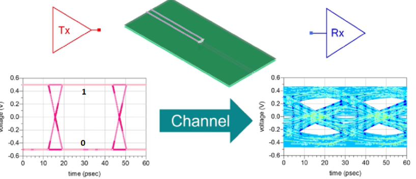
2.4 High-Speed Signal Routing Challenges
As signal frequencies increase, PCB traces behave like transmission lines, leading to signal degradation due to skin effect, dielectric losses, and propagation delays.
Solution:
- Keep high-speed traces as short and direct as possible.
- Use microstrip or stripline configurations for controlled impedance.
- Avoid sharp bends (use 45° or curved traces instead of 90° turns).
- Match trace lengths for differential pairs to prevent skew.

3. Best Practices for Ensuring Signal Integrity
3.1 Proper Stackup Design
A well-designed PCB stackup ensures controlled impedance and minimizes EMI. Key considerations include:
- Use multiple ground planes to provide low-impedance return paths.
- Place high-speed signal layers adjacent to ground planes for shielding.
- Select dielectric materials with stable properties over frequency (e.g., FR4, Rogers).
3.2 Termination Techniques
Proper termination prevents signal reflections in high-speed lines:
- Series termination (at the source) for point-to-point connections.
- Parallel termination (at the load) for distributed loads.
- AC termination for reducing high-frequency ringing.
3.3 Differential Pair Routing
Differential signaling (e.g., USB, HDMI, PCIe) improves noise immunity:
- Route differential traces symmetrically with matched lengths.
- Maintain consistent spacing between pairs to avoid mode conversion.
- Avoid vias and discontinuities in differential paths.
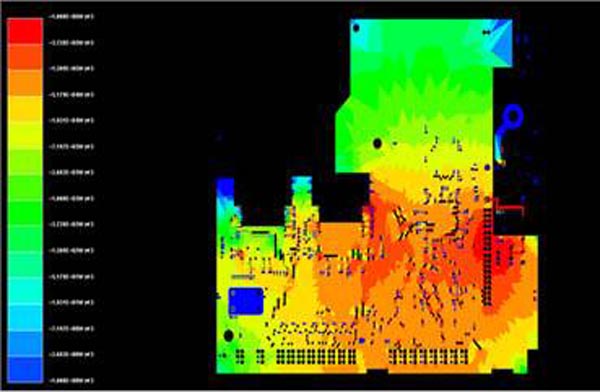
3.4 Simulation and Analysis
Before fabrication, use simulation tools (e.g., HyperLynx, ADS, Sigrity) to:
- Perform signal integrity analysis (eye diagrams, TDR).
- Simulate power integrity to identify voltage drop and noise issues.
- Analyze crosstalk and EMI to optimize layout.
3.5 EMI Mitigation Strategies
EMI can disrupt signal integrity and cause compliance failures:
- Use proper grounding techniques (star grounding for mixed-signal designs).
- Implement shielding (copper pours, ferrite beads).
- Follow FCC/CE guidelines for high-frequency designs.
4. Advanced Techniques for High-Speed PCB Design
4.1 Via Optimization
Vias introduce impedance discontinuities and inductance. To minimize their impact:
- Use blind/buried vias for dense designs.
- Place ground vias near signal vias to shorten return paths.
- Avoid excessive via stubs in high-frequency signals.
4.2 Signal Conditioning
For long traces or high-loss materials:
- Use pre-emphasis (boosting high frequencies at the transmitter).
- Apply equalization (compensating for losses at the receiver).
4.3 3D Electromagnetic Simulation
For complex RF/microwave designs, 3D EM solvers (e.g., HFSS, CST) help analyze:
- Antenna effects in high-speed traces.
- Parasitic coupling in multi-layer boards.
5. Conclusion
Signal integrity is a fundamental requirement in modern PCB design, especially for high-speed digital and RF applications. By addressing impedance mismatches, crosstalk, power noise, and routing challenges, engineers can ensure reliable signal transmission.
Key takeaways include:
- Maintain controlled impedance through proper stackup and trace design.
- Use differential pairs and termination to reduce noise and reflections.
- Simulate designs before fabrication to identify and fix SI issues.
- Follow best practices in grounding, shielding, and EMI reduction.
By implementing these strategies, PCB designers can achieve optimal signal integrity, leading to faster, more reliable electronic systems.