IC Substrate PCB
Since technology evolution is going on, everything is becoming smart and gadgets are becoming smaller.
For smart devices require a smart solution that can hold things together for a seamless behavior.
Therefore, Integrated Circuit substrates partake a shot of prominence at the current technological evolution.
By the emergence of various types of ICs, for example, child-scale package (CSP) and ball grid package (BGP).
The IC substrates are the key for these IC packages as novel package carriers and accounted for it.
Certain IC package substrates are important for designing electronic chip sets and the electronic designers highly recommend them.
The manufacturing process of IC substrate should be comprehended for the proper functional role-play of modern electronics and their applications.
The demand for IC substrate is booming due to its apprehension of the advanced PCB (Printed Circuit Board).
Almost all the applications require to be paired with the layers of HDI PCB and flex-rigid PCBs
That are highly popular among the telecommunications and electronics niche.

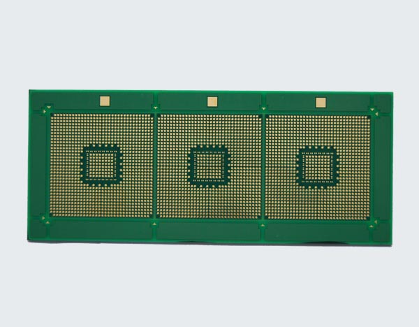
6Layers PCB Thickness: 0.7mm
BGA 0.3mm VIA In Pad ,
Line width / space : 2.5 mil/2.5mil
IC substrate is the base of the IC packages.
It is utilized as the baseboard in the package of bare integrated circuit chips.
The substrate IC is crucial to connect the chip and circuit board,
Where IC remains to an intermediate product with the functions below:
- Captures semiconductor IC chip
- Connects the chip and PCB with the insider routing
- Shields strengthens and provides support to the IC chip through thermal dissipation tunnel
ICs can be described as electronic devices of micro-scale.
Different components like indicator, capacitor, resistor and,
Diode are intertwined collectively through the process and fabricated the chip of semiconductor.
It is also popularly known as substrate and then encapsulated within a shell to,
Form a microstructure and includes all the functions to make sure seamless performance.
IC substrate plays a vital role as the connector of the PCBs to the semiconductor chip.
It is like the channel that is important to hold the capacity on IC fabricators.
The interconnection densities will have the support to surpass the PCB fabricators while the IC substrate is manufactured.
Even manufacturers need this for possessing to prove the specialty and solutions in chemical expertise related to the high-density designs.

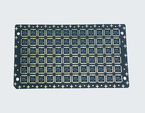
2 Layers Material: BT
PCB Thickness: 0.2 mm
VIA In Pad ,
Line width / space : 2 mil/2mil (0.05mm)
ICs act as a transitional product that helps to capture the semiconductor IC chip.
It directs towards the link to the chip with the PCB.
This is done to ensure protection, support well as maintain the strength of the IC chip that will be moved by the thermal dissipation tunnel.
All the components are attached and featured with:
- Compact circuit:
Being an integrated circuit, the IC has been manufactured in a certain way that keeps the design,
Installation, and debugging processes simple and uniform. - Cost-efficient:
Compared to the other distinct components,
The IC is the most cost-efficient solution that has a higher performance rate. - Consistency:
The entire circuit and performance are highly consistent and reliable.
The soldering joints have been condensed to a greater extent in ICs.
It makes it convenient for virtual welding that also can be reduced and makes the IC more reliable. - Productive:
The biggest advantage is being productive because the ICs consume lesser power in a smaller volume.
The random circuits consume less power and comprise with lower power failure rate than the IC substrates.
ICs have advantages over discrete electronic circuits, such as low weight, less wiring, and high durability.
All the advantages are best suited for mass production based on diversified classification.
The IC substrates are diversified and fall under different classifications,
That comprehend to be better and enact by the classifications among each type and class.

2 Layers Material: BT
PCB Thickness: 0.2 mm
VIA In Pad ,
Line width / space : 2 mil/2mil (0.05mm)
The IC substrates are classified based on three things:
package type, material type, and bond technology types.
Below these major types of IC has been explained:
- Classification based on Package Type:
The materials of the IC packaging are surrounded by the circuit material to protect it from corrosion or physical damage that enables mounting of the electrical contacts that connect through the PCB. The types are:
BGA IC Substrate:
IC is best suited for operating in thermal dissipation to enhance performance.
The electrical performance needs to be highly exceptional by increasing the chip pins and being suitable for IC packages with more than 300 pins.
CSP IC Substrate:
CSP is considered a single packaged chip that is lightweight, small, and works similarly to ICs.
CSP IC substrate is typically used in memory products, the telecommunication industry,
And other electronic devices that require a small number of pins on-chip.
FC IC Substrate:
Flip Chip (FC) is another type of packaging with flipping chip features with low signal interference,
Low circuit loss, good performance, and effective heat dissipation.
MCM IC Substrate:
MCM is a multi-chip module that integrates with the IC substrate and,
Absorbs the chips to function differently into a single package.
This makes the product optimal in performance due to its attributes of being short,
lightweight, thin, and compact. Most of the chips are packaged in a single package therefore,
This type of substrate is unable to perform well under signal interference, heat dissipation, fine wiring, etc.
- Classification based on Material Types:
Materials are important as IC packages rely upon their chemical, electrical, and material combination.
It differs in functionalities, lead-frame,
And lamination that prevails the material composition using silver or golden wire-bond finishes.The types of materials are: - Rigid IC Substrate:
This type of IC is made of epoxy resin, ABF resin, and BT resin.
It requires to have the Coefficient of Thermal Expansion (CTE) in between 13 to 17 ppm per degree Celsius. - Flex IC Substrate:
This type of IC is made by PE or PI resin and the CTE should remain between 13 to 27 ppm per degree Celsius. - Ceramic IC Substrate:
This type of IC substrate is made of ceramic materials,
such as silicon carbide, alumina, aluminum nitride, and aluminum oxide.
The CTE could be relatively low in this maintaining to be in 6 to 8 ppm in per degree Celsius.
- Classification based on Bond Technology Types:
The ICs should be protected from damages to the external factors so they can redistribute the inputs and outputs in a manageable fine pitch.
The bond technology comes to help to standardize the structure so it can be directed to the thermal pathway.
The basic types of bond technology are classified in:
– Wire Bonding
– FC Bonding
– Tape Automated Bonding (TAB)
The last step in semiconductor devices production requires to have protection by the casing.
This protects from the damages in detrimental external elements or age-related corrosion.
The design of the casing safeguards and blocks disproportions besides promoting electrical contracts while delivering signals to the device circuit board.
The design of the IC packaging is different from categorization depending on formation including the substrate type and the lead-frame type.
The IC packaging designs are formed in both primary and secondary categorization that includes multiple types of packaging:
- Pin-grad array that becomes deployed and socketing
- Lead-frame packages and dual-inline
- The packages are used for assemblies requiring pins to go through holes
- Chip scale package directs to the surface mountable single-die package.
The diameter is 1.2 times smaller than the die. - Quad flat pack is a leadless type packaging that has a lead frame.
- Quad flat no-lead is a small package that is close to resembling the chip size and deployed for surface mounting primarily.
- Multichip packaging is referred to as multichip modules that integrate discrete components,
semiconductor dies, and multiple ICs onto a substrate. It also resembles a bigger IC in a multichip package. - Area array package provides maximum performance and conserves space
By utilizing the rest of the space in the chip surface for interconnection.
Most of the companies use the area of an array package that is required for multichip structures
Because these packages and modules present leading options and solutions that can utilize the system-on-chip format.
The ideal IC with correct substrate and packaging helps to consider these features to keep things safe and protected.
Copper plating solutions enable high reliability in IC packaging and enable better compatibility with the desired dielectric.
IC packaging is a cost-effective solution that also offers:
- Promotes better adhesion and intensifies surface treatments
- Makes the dielectric layer conductive with electroless copper seed deposition
- Enhances reliability by electrolytic plating through the fill, copper pillar, and redistribution layers (RDL)
Specialized in pure copper plating makes it reliable to interconnect on substrates for ball grid arrays (BGA) and chip-scale packages (CSP).
High throwing power is highly important for distributing excellent thickness.
The coverage over the substrates is a complex geometry provides the highest degree of reliability along with:
- Advantage of wet chemistry of low cost and better performance
- Optimizes the device performance according to the choice of standard options or tailored individualized recipes
IC substrates PCB has been produced on BGA architecture and manufactured in a similar process.
The main connection remains between the PCB and IC chip through the network of conductive holes and traces.
The precision has improved and it has created differences between IC substrate board and PCB in material design,
Equipment, selection, post-process, and so on.
Due to some critical functions of IC substrates, it requires to consist of protection and circuit support,
Power distribution, signal distribution, and heat dissipation.
- IC substrate manufacturing:
The key component of IC substrate PCB consists of packaging so it can be replaced into some lead frame applications.
If you compare with standard PCB, IC substrate may face some difficulties of high performance and advanced function in manufacturing.Therefore, IC substrates represent a high miniaturization level of the PCBs manufacturing process that includes similarities of semiconductors.
It is usually a thin layer and easy to deform and bulge if the board has a thickness of 0.2mm.Such difficulty has solutions by shrinking the board, positioning the system layers, laminating parameters, etc.
The warpage of substrate and thickness of lamination are controlled effectively. - Microvia manufacturing:
This technology has many aspects. First, a conformal mask that is compensated
By the laser drilling through the opening and blind hole will be located directly through the aperture.
Then laser drilling micromachining comprises through-hole shape, aspect ratio, and side etching.
Lastly, copper plating filling technology has a blind hole that has aspects as through-hole filling ability,
Blind hole opening, sinking, copper plating reliability, and so on. - Copper plating and patterning:
It is correlated with different technological aspects that have control and circuit compensation technology,
Uniform control for the thickness of copper plating, and fine line fabrication technology. - Solder mask:
For IC substrate PCB, a soldering mask is effective.
It consists of printing and hole filling technologies and,
Enables less than 10 micrometers of substrate height difference through pad and solder mask.
It is not recommended for more than 15 micrometers. - Surface finishing:
It is emphasized for a uniform thickness on IC substrate PCBs and ENIG and ENEPIG is acceptable. - Reliability and inspection tests:
The equipment is used for IC substrate PCB that is different than ordinary PCBs.
It must be capable of having mastered skills for inspection of the PCBs have dedicated modern equipment.
The characteristics of IC substrates are advantageous and offer lower facilities and mass production.
It is utilized in civilian and industrial electrical and electronic equipment,
Such as cassette recorders, computers, televisions as well as in space, remote-control,
Communication devices, military applications, and so on.
The major difference between the PCB and IC is stated in the chip integration on the computer motherboard.
Once IC is damaged, the entire chipset should be changed.
Small or big, every almost all electronic devices require PCBs and IC is the most integral part that is used as miniaturized electronic circuits.
Every lightweight, powerful electronic devices like smartphones, laptops, tablets and networks,
Telecommunications, medical, industrial control, aerospace, and military field.
The core fields of applications for IC substrate PCB include CPU,
North-South Bridge chip, graphics card, memory chip, communication chip, game machine, etc.
