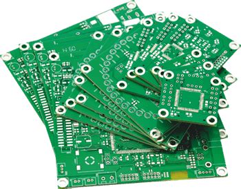
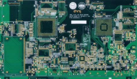
Implementation of conductive hole plugging process
For surface mount boards, especially BGA and IC mounting, the via plugging requirements must be flat, with a convex and concave of plus or minus 1mil, and the via edge must not be red and tinned; the via hole must not have tin beads. In order to meet customer requirements, the via plugging process can be said to be varied, the process flow is particularly long, and the process control is difficult. There are often problems such as oil loss during hot air leveling and green oil solder resistance experiments; oil explosion after curing. Now, according to the actual production conditions, various PCB plugging processes are summarized, and some comparisons and explanations are made in the process and advantages and disadvantages:
Note: The working principle of hot air leveling is to use hot air to remove excess solder on the surface and holes of the printed circuit board, and the remaining solder is evenly covered on the pads and unresisted solder lines and surface packaging points. It is one of the surface treatment methods of printed circuit boards.
1.Plug hole process after hot air leveling
This process flow is: board surface solder mask → HAL → plug hole → curing. The non-plugging process is used for production. After hot air leveling, aluminum sheet screen or ink blocking screen is used to complete the plugging of all the vias required by customers. The plugging ink can be photosensitive ink or thermosetting ink. Under the condition of ensuring the consistency of wet film color, the plugging ink is preferably the same ink as the board surface. This process can ensure that the vias do not drop oil after hot air leveling, but it is easy to cause the plugging ink to pollute the board surface and make it uneven. Customers are prone to cause cold solder joints (especially in BGA) during mounting. Therefore, many customers do not accept this method.
2.Plug-in process before hot air leveling
2.1 Use aluminum sheet to plug holes, solidify, grind the board, and then transfer the pattern.
This process uses a CNC drilling machine to drill out the aluminum sheet to be plugged, make a screen, and plug the holes to ensure that the vias are full. The plugging ink can also use thermosetting ink. Its characteristics must be high hardness, small resin shrinkage change, and good bonding with the hole wall. The process flow is: pre-treatment → plugging → grinding → pattern transfer → etching → board surface solder mask.
This method can ensure that the via plugging is flat, and the hot air leveling will not have quality problems such as oil explosion and oil loss on the hole edge. However, this process requires one-time thickening of copper to make the copper thickness of the hole wall meet the customer’s standard. Therefore, it has high requirements for the copper plating of the whole board and the performance of the grinding machine to ensure that the resin on the copper surface is completely removed and the copper surface is clean and not contaminated. Many PCB factories do not have a one-time thickening copper process, and the performance of the equipment does not meet the requirements, resulting in this process not being used much in PCB factories.
2.2 Directly screen-print the board surface solder mask after plugging the hole with aluminum sheet
This process uses a CNC drilling machine to drill out the aluminum sheet to be plugged, make a screen, and install it on the screen printer for plugging. After the plugging is completed, it should not be parked for more than 30 minutes. Use 36T screen to directly screen-print the board surface solder mask. The process flow is: pre-treatment – plugging – screen printing – pre-baking – exposure – development – curing
This process can ensure that the via cover oil is good, the plugging is flat, and the wet film color is consistent.
After hot air leveling, it can ensure that the via is not tinned and there are no tin beads in the hole. However, it is easy to cause the ink in the hole to be on the pad after curing, resulting in poor solderability; after hot air leveling, the edge of the via will bubble and lose oil. It is difficult to control the production using this process method. The process engineering personnel must use special processes and parameters to ensure the quality of the plugging.
2.3 After the aluminum sheet plugs the hole, develops, pre-cures, and grinds the plate, the board surface solder mask is performed.
Use a CNC drilling machine to drill out the aluminum sheet that requires plugging holes, make a screen, and install it on a shift screen printer for plugging holes. The plugged holes must be full and protruding on both sides. After curing, grind the board for board surface treatment. The process flow is: pre-treatment – plugging holes – pre-baking – development – pre-curing – board surface solder mask
Since this process uses plugging hole curing to ensure that the vias will not drop oil or explode after HAL, but after HAL, it is difficult to completely solve the problem of tin beads in the vias and tin on the vias, so many customers do not accept it.
2.4 Board surface solder mask and plugging holes are completed at the same time
This method uses a 36T (43T) screen, installed on a screen printer, and uses a pad or nail bed to plug all the vias while completing the board surface. The process flow is: pre-treatment-screen printing-pre-baking-exposure-development-curing
This process flow is short in time and has high equipment utilization. It can ensure that the vias do not drop oil and the vias do not get tin after hot air leveling. However, due to the use of screen printing for plugging holes, a large amount of air is stored in the vias. During curing, the air expands and breaks through the solder mask, causing voids and unevenness. Hot air leveling will have a small amount of tin in the vias. At present, after a large number of experiments, our company has selected different types of inks and viscosities, adjusted the pressure of screen printing, etc., and basically solved the via voids and unevenness. This process has been used for mass production.