Introduction to SMT patch process
Surface Mount Technology (SMT) is an assembly technology that directly mounts electronic components on a printed circuit board (PCB). Compared with traditional through-hole technology (THT), SMT has the advantages of higher assembly density, smaller volume, shorter delivery cycle and lower cost. This article will give a detailed introduction to the SMT patch process.
1.Overview of SMT patch process
The SMT patch process mainly includes the following steps: printing, patch, welding and testing. The following is a brief introduction to each step:
Printing: Printing solder paste on the PCB to prepare for subsequent patch and welding.
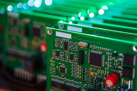
Patch: Mount electronic components on the PCB.
Welding: Connect electronic components to the PCB through molten solder.
Detection: Test the assembled circuit board to ensure that its function and appearance meet the requirements.
2.Detailed explanation of SMT patch process flow
Printing
Printing is the first step in the SMT patch process flow, which mainly involves the application of solder paste. Solder paste is a paste-like substance composed of solder powder, organic carrier and other additives, which is used to connect components to PCB. There are many ways of printing, such as screen printing, dispensing and jetting. During the printing process, it should be ensured that the solder paste is evenly applied to the pads of the PCB and the amount of solder paste is controlled to prevent too much or too little.
Patching
Patching is the second step in the SMT patch process flow, which mainly involves mounting electronic components on the PCB. Patching can be done manually or automatically. In automatic patching, a patch machine is used to place components on the PCB according to a preset program. In manual patching, the operator uses a microscope and a vacuum pen to place components on the PCB. During the patching process, it should be ensured that the components are placed accurately without misalignment and tilting.
Welding
Welding is the third step in the SMT patch process flow, which mainly involves connecting electronic components to the PCB. Welding is usually carried out by hot air welding or laser welding. In hot air welding, a hot air gun is used to melt the solder and connect the components and pads. In laser welding, a laser beam is used to melt the solder and connect the components and pads. During the welding process, the temperature and time should be controlled to prevent damage to the components or the occurrence of phenomena such as cold soldering and cold soldering.
Detection
Detection is the last step in the SMT patch process flow, which mainly involves the detection of the assembled circuit board to ensure that its function and appearance meet the requirements. Detection is usually carried out by automatic detection or manual detection. Automatic detection uses detection equipment to detect the circuit board, while manual detection is performed by the operator using tools such as test equipment and microscopes. During the detection process, the electrical performance, mechanical performance and appearance quality of the circuit board should be checked to see if they meet the requirements. If problems are found, timely measures should be taken to repair or adjust them to ensure the quality and reliability of the final product.
3.Development trend of SMT patch process
With the rapid development of the electronics industry and technological progress, the SMT patch process is also constantly developing and improving. The development trend of SMT patch technology in the future includes the following aspects:
High-density integration: With the improvement of the functions and performance of electronic products, higher integration is required to meet the demand. Therefore, high-density integration will become an important development direction of SMT patch technology. High-density integration can achieve advantages such as smaller volume, shorter wiring distance and higher transmission speed.
Green environmental protection: With the improvement of environmental awareness, green environmental protection has become an important development direction of the electronics industry. In the SMT patch process, environmentally friendly materials and processes should be used to reduce the generation of waste and pollutants, while strengthening recycling and reuse work to promote sustainable development.
Intelligent manufacturing: Intelligent manufacturing is an important development direction of modern manufacturing. In the SMT patch process, automation and intelligent technology should be used to achieve the goals of automated control, real-time monitoring and intelligent optimization of the production process, and improve production efficiency and product quality.
Customized production: With the diversification of consumer demand, customized production has become an important trend in the electronics industry. In the SMT patch process, a customized production method should be adopted to carry out customized design and production according to customer needs to meet the needs of different customers and market changes.
Application of artificial intelligence and big data technology: Artificial intelligence and big data technology can help companies better understand market demand, optimize production processes and improve product quality. In the SMT patch process, artificial intelligence and big data technology should be used to analyze and process production data, identify problems and propose improvement measures to improve production efficiency and product quality.
In short, with the rapid development and technological progress of the electronics industry, the SMT patch process will continue to develop and improve. In the future, the SMT patch process will pay more attention to the development trends of high-density integration, green environmental protection, intelligent manufacturing, customized production, and the application of artificial intelligence and big data technology. These development trends will help improve production efficiency and product quality, meet market demand and promote the electronics industry.