
Key points of precision graphic transfer technology control
I. High-density FPC flexible circuit graphic transfer process control technology
In the high-density FPC flexible circuit manufacturing process, graphic transfer is a key control point and a technical difficulty. Its quality directly affects the qualified rate of FPC flexible circuits. Therefore, in the production process, the following points must be achieved:
- The dry film is as flat as possible and the thickness is uniform. The dry film is required to have good flexibility, good plasticity, fluidity and adhesion to ensure gapless film lamination.
- Exposure should be moderate. In this way, the lines can be clear and straight, and the qualified rate of graphic electroplating and the electrical properties and other process requirements of the substrate can be guaranteed.
- Development should be sufficient. Development is an important process directly connected to the next process. The quality of development is an important indicator of the success of the entire graphic transfer.
II. In the process of high-density image transfer, if the control fails, it is very easy to have quality problems such as infiltration, poor development or anti-corrosion dry film peeling.
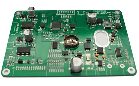
In order to further understand the cause of the failure, this phenomenon is analyzed:
- Penetration: The so-called penetration is that the dry film is not firmly bonded to the surface of the copper clad board, allowing the plating solution to penetrate deeply, causing the “negative phase” part of the plating layer to become thicker and the plated tin-lead anti-corrosion layer to cause problems in etching. It is easy to cause the scrapping of printed circuit boards, which is a key point that needs special attention in production. The reasons for the penetration caused by the graphic electroplating process are analyzed as follows:
(1) The dry film has poor developability and is overused.
The photoresist dry film mentioned above has a structure composed of three parts: polyester film, photoresist film and polyethylene protective film. Under ultraviolet light, the dry film and the surface of the copper clad board have good adhesion, which plays a role in resisting electroplating and etching. If some films are used beyond the validity period, this layer of adhesive will fail, and the protective effect will be lost during the electroplating process after the film is attached, resulting in penetration. The solution is to carefully check the effective use cycle of the dry film before use.
(2) The influence of temperature and humidity on film lamination:
Different dry films have more suitable lamination temperatures. If the lamination temperature is too low, the anti-corrosion film cannot be fully softened and properly flowed, resulting in poor bonding between the dry film and the surface of the copper-clad laminate; if the temperature is too high, bubbles will be generated due to the rapid volatilization of the solvent and other volatile substances in the anti-corrosion agent, and the dry film will become brittle and not resistant to electroplating, resulting in warping and peeling, causing infiltration and scrapping. The Wuxi DFP type and the American DuPont 3000 type dry films currently used generally control the lamination temperature to be 70-90℃.
The dry film used is water-soluble, and the humidity in the air has a greater impact on it.
When the humidity is high, the adhesive of the dry film can achieve a good bonding effect when the lamination temperature is low. In particular, the summer temperature in the southern region is relatively high. From long-term practice, a set of better temperature control parameters has been explored. Under the condition of 20-25℃, when the relative humidity is above 75%, the film-pasting temperature is preferably below 73℃; when the relative humidity is 60-70%, the film-pasting temperature is preferably 70-80℃; when the relative humidity is below 60%, the film-pasting temperature is preferably above 80℃. Similarly, increasing the pressure and temperature of the film-pasting rubber roller also achieves better results.
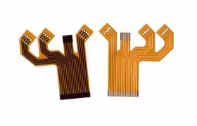
(3) Too long exposure time or insufficient exposure:
Under ultraviolet light, the photoinitiator that absorbs light energy decomposes into free radicals to initiate monomers for photopolymerization reaction, forming bulk molecules that are insoluble in dilute alkali solutions.
To achieve the best polymerization effect for each dry film, there must be an optimal exposure amount. From the definition formula of light energy, it can be seen that the total exposure amount E is the product of light intensity I and exposure time T. If the light intensity I remains unchanged, the exposure time T is an important factor that directly affects the total exposure amount. When the exposure is insufficient, due to incomplete polymerization, the film swells and softens during the development process, resulting in unclear lines or even film shedding, causing poor bonding between the film and copper; if the exposure is excessive, it will cause development difficulties, and will also cause warping and peeling during the electroplating process, forming seepage plating. Therefore, the solution is to strictly control the exposure time. Each type of dry film should be measured according to the process requirements when it is used. For example, if a Swisston 21-level wedge meter is used, the level difference is 0.15, and it is appropriate to control 6-9 levels.
(4) Poor development:
After the copper-clad laminate with the dry film attached is exposed, it must be developed by a developer. The unexposed dry film is kept in its original composition and reacts with the developer in the developer as follows:
-COOH+Na+ —COONa+H+
Among them, —COONa is a hydrophilic gene, soluble in water, and peeled off from the dry film, so that the entire board surface reveals the pattern to be electroplated, and then electroplating is carried out. —COONa is the dry film component, and Na+ is the main component of the developing solution (Na2CO3 3% plus an appropriate amount of defoaming agent). If the development is not good, there will be residual glue on the pattern conductor part, which will cause the copper to not be plated locally, resulting in waste and defective products. This is the most common quality problem in the development stage. The reasons are:
(5) The exposure time is too long.
When the exposure is excessive, the ultraviolet light passes through the transparent part of the photographic film and produces refraction and diffraction phenomena, irradiating the dry film under the opaque part of the photographic film, so that the part of the dry film that should not have photopolymerization reaction will be partially exposed and undergo polymerization reaction. When developing, residual glue and excessively thin lines will be produced. Therefore, proper control of exposure time is an important condition for controlling the development effect.
At the same time, during mass production, it should also be noted that when the ultraviolet light tube is in operation for a long time, the temperature rise and the heat radiation are large, and a similar effect similar to ultraviolet irradiation occurs on the dry film under the film, causing the dry film to polymerize, also known as thermal polymerization reaction. For this reason, this requires that the exposure machine should have a cooling device.
(6) The contrast of the photographic film is not enough.
The quality of the photographic film can be expressed by optical density: the black part of the film has a high optical density; the transparent part has a low optical density. The greater the difference between the two, the better the contrast is, which is called good contrast. If the contrast of the photographic film itself is not enough, it will directly affect the control of the exposure time. If the optical density of the opaque part of some positive films used for graphic transfer is not high enough, it will directly affect the dry film under the cover and will also undergo obvious photopolymerization reaction, and produce a large area of residual glue. Therefore, the quality of the photographic film must be strictly controlled.
III. The influence of developer and developer on the quality of development: When using the developer of American King Engraving Company.
The main component of the developer is 3% sodium carbonate (add an appropriate amount of defoaming agent), the spray pressure of the developer is 1.8-2KGF/CM2, the temperature of the developer is 28-32℃, and the development time is adjusted to expose copper through 1/2 of the development area.
If the developer concentration is too low, the development speed is slow; if it is too high, the solidified graphics will be damaged or even fall off. Therefore, the concentration of the developer should be strictly controlled by measuring the pH before each production; if the spray pressure is insufficient, the surface of the dry film will not be rinsed clean, resulting in residual glue; if the pressure is insufficient, a large number of bubbles will be generated, which will reduce the effective concentration of the sprayed sodium carbonate, and the reaction will not be complete, resulting in residual glue; if the developer temperature is too low, it will also cause the sodium carbonate to react incompletely with -COOH, resulting in residual glue. It should be mentioned in particular that when developing fine wire graphics, try to use a low spray pressure and shorten the development time. After development, you can use a 1% sodium carbonate solution and use soft foam plastics to gently scrub along the line direction, and finally use a high-pressure water pump to clean.
In short, strictly controlling the required process conditions can ensure high quality development. Make the obtained fine graphics more reliable and stable. This is just a matter of experience, and more effective process methods and operating skills must be explored based on the process equipment and process level of the enterprise.