Andwin Circuits PCB Products Provide you with better service
High quality Complex PCB manufacturing
From PCB prototype to volume production
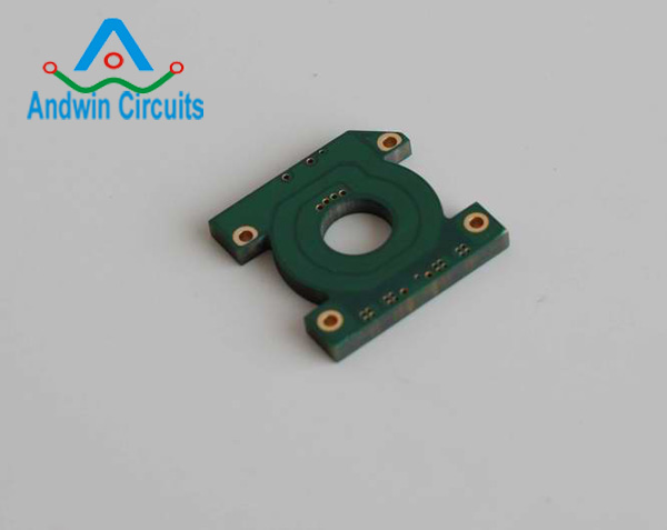
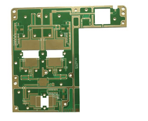
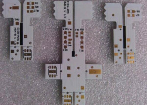
6 Layers PCB
6 layers , 2 steps HDI PCB (2 + 2 + 2 ) ,BGA 0.18mm, material : ITEQ IT180A
Half plating holes
Application: wireless communication module
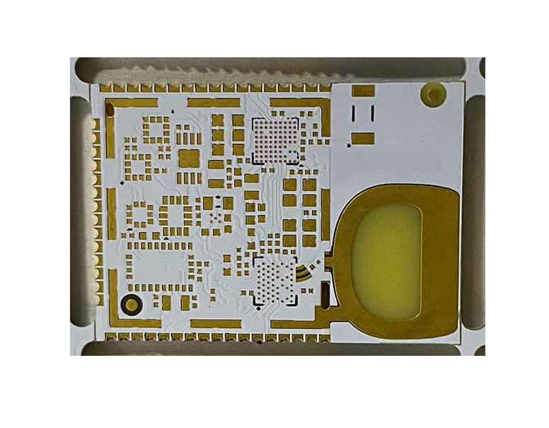
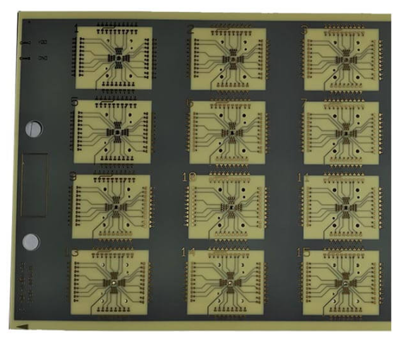
36 Layers PCB
36 layers , 2 steps HDI PCB , material : ShengYing S1000-2
Application: Chip TEST board
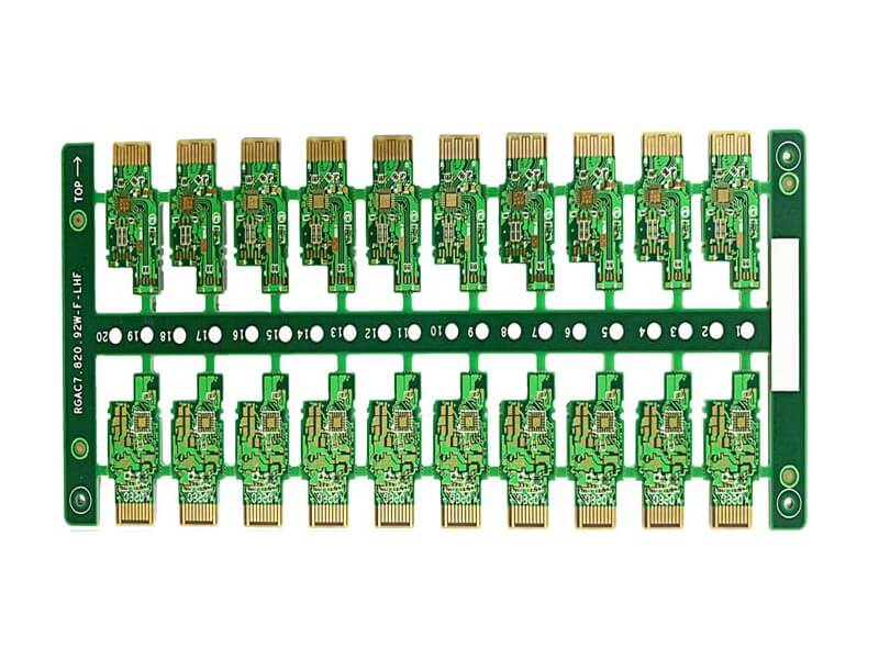
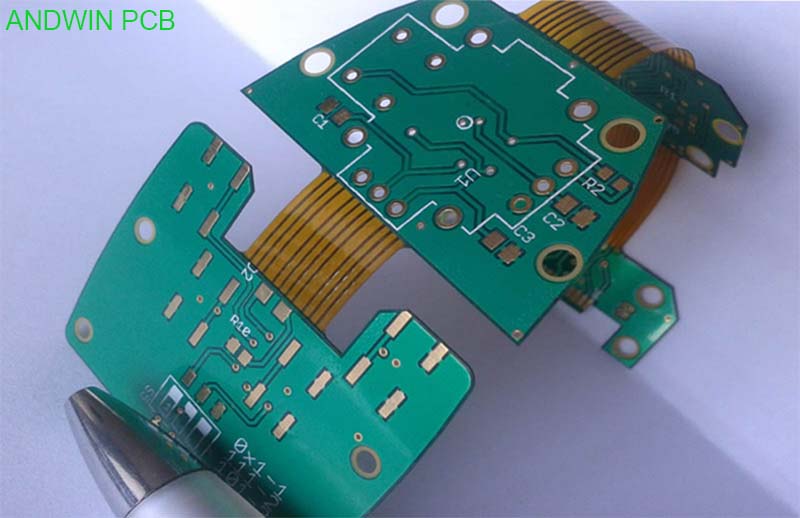
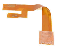
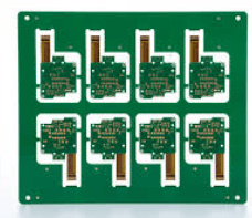
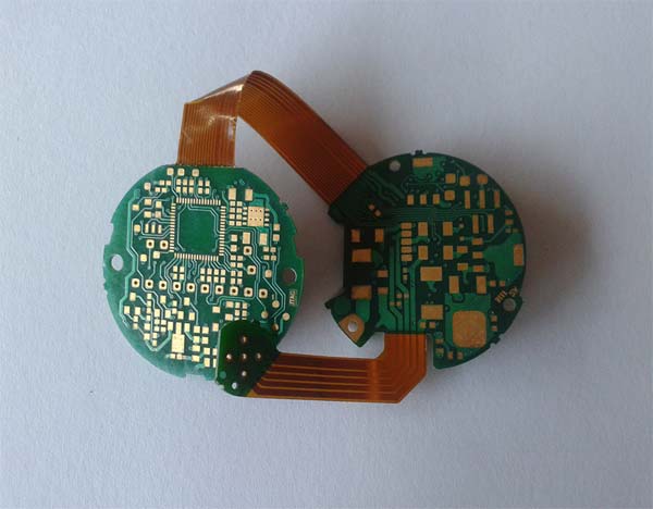
Rigid flex pcb
- Rigid flex PCB Prototype and production manufacturing
- Meet your special and complex technical requirments
- Reasonable & good price
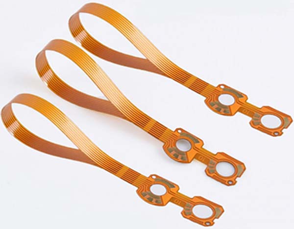
Flex PCB
Flex PCB from 1 to 8 layers
( samples up to 12 layers )
Also, provide many types Flex PCB with special requirement.
Min. trace width / space : 0.05/0.05mm,
Max. Copper thickness: 3 OZ ( 0.105mm )
Get reaction in 1 hour, fast delivery FPCB in 3 days.
High Frequency PCB
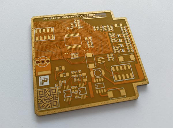
- Well know RF circuits boards design
- Ready raw material in stock ( Lead time short ).
- Strong Process capability (Track:3/3mil,6mil Via holes)
- Technology support from strongly team
- Reasonable cost
Megtron 6 High Speed Multilayer PCB
- We only use the highest quality raw materials to make your Megtron 6 High speed PCB.
The raw material for your Megtron 6 High speed PCB is imported from Japan and USA
especially electroplating and solder mask. - Panasonic Megtron 6 raw material keep safety stock,which is ensure you to get Megtron 6 high speed PCB faster.
- Design rule check ( DRC ) – all of your megtron 6 High speed PCB will be done DRC before production line, so that, ensure your PCB have no accident in PCB design.
- Low moisture absorption
- Tightly controlled DK
- Low DF
- UL 94 VO rating
- For low layer count microwave designs
TU-872 SLK Sp High Speed PCB
- Dielectric constant less than 3.5
- Dissipation factor less than 0.010
- Excellent, stable and flat Dk/Df performance
- Compatible with most FR-4 processes
High TG PCB SH260 polymide PCB?
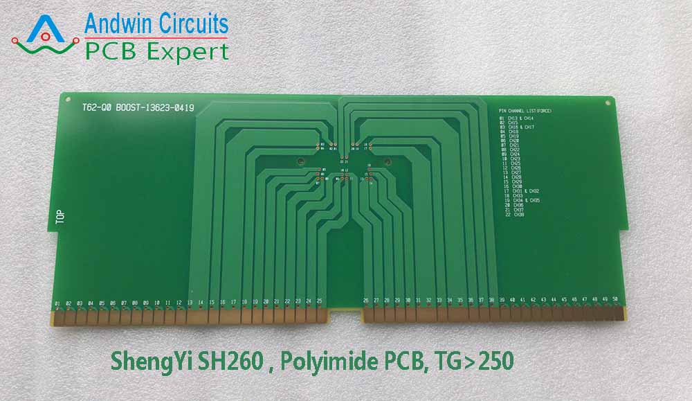
SH260 is rigid polyimide PCB raw material by ShengYi Technology,
sh260 laminate TG >250 C,Thickness 0.05mm – 3.2mm.
ShengYi SH260 is High Performance, Polyimide Laminate and Prepreg PCB raw material.
- Polyimide system
- Ultra-high thermal performance
- Tough resin system, Non-MDA chemistry
- Low moisture absorption
- Maintain mechanical strength
- Bonding strength at high temperature
- Halogen-free, chemistry and lead-free compatible
ISOLA 370HR High TG PCB
- Tg: 180°C (DSC)
- Td: 340°C (TGA @ 5% wt loss)
- Low CTE for reliability
- T260: 60 minutes
- T288: 30 minutes
- RoHS Compliant
- Thickness: 0.002″ (0.05 mm) to 0.125″ (3.2 mm)
- IPC-4101D WAM1 /98 /99 /101 /126
- UL – File Number E41625 as PCL-FR-370HR
ISOLA IS410 PCB
ISOLA IS410 PCB raw material is TG180 high reliability PCB material
Tg: 180°C
Td: 350°C
Dk: 3.97
Df: 0.0200
ISOLA IS420 PCB
ISOLA IS420 PCB raw materialis a high performance
170°C glass transition temperature (Tg) FR-4 system ,
It is for multilayer Printed Wiring Board (PWB) applications
where maximum thermal performance and reliability are required.
Tg 170, Td 350
Dk 4.04, Df 0.021
/98 /99 /101
Copper coin pcb
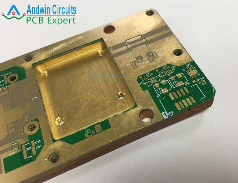
- High thermal conductivity.
- Copper coin PCB comprises the conductive traces of a PCB with high thermal conductivity
- Excellent heat dissipation performance
- Suitable for extreme environments
- Enhanced electrical connection and mechanical stability
- Design flexibility and
Copper inlay pcb
Copper inlay PCB Capability
- Copper Inlay Shape: “I”,“U”,“T”
- Copper Inlay Size Min.: 3mm*3mm
- Copper Inlay Thickness Max.: 6.0mm
- PCB thickness Max.: 12mm
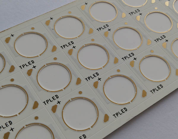
Metal Core PCB

Ceramic PCB
Andwin PCB provide Ceramic PCB manufacturing since 2010,
Our ceramic PCB material include Alumina(Al2O3), Aluminum nitride(AIN ALN), Silicon nitride (SIN), Beryllium Oxide (BeO), Boron Nitride (BN), Silicon Carbide (SiC) ,Zirconia ( ZrO2 ) etc.
The ceramic PCB manufacturing technical use DPC, DBC, Thick film and AMB.
Andwin have strongly ceramic PCB manufacturing capability to match your requirement.
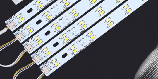
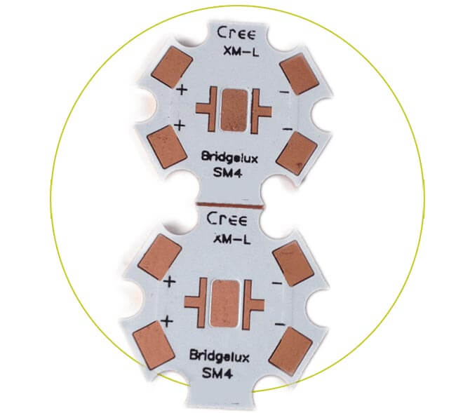
1 layers aluminum metal core pcb for led strip lighting
1 layers aluminum metal core pcb for led strip lighting
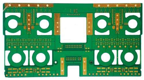
12 layers heavy copper pcb for power source
12 layers heavy copper pcb for power source
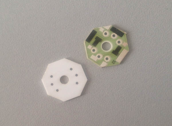
2 layers ceramic pcbs for sensor
2 layers ceramic pcbs for sensor
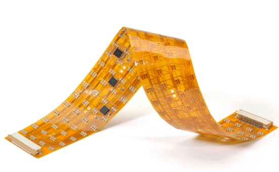
2 layers flexible pcb for led lighting
2 layers flexible pcb for led lighting
2 layers metal core pcb for led lighting
2 layers metal core pcb for led lighting
6 layers rigid flex hdi pcb circuit boards
6 layers rigid flex hdi pcb circuit boards
6 layers rigid flexible pcb for watch
6 layers rigid flexible pcb for watch
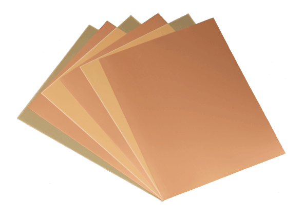
roger pcb material
roger pcb material
FAQ about Andwin printed circuit boards
Below we have listed some of the most common questions we receive and everyday discussion topics. You can also ask your PCB question here.