Main Trends and Technologies of PCB Sequential Lamination
The trend of utilizing electronic products is the driving force for generating more technological innovations. With the development of the times, electronic innovations have also become smarter over time. Electronic devices are meeting their needs in various fields from home to rocket technology.
As the demand graph reaches its peak, the market competition is getting closer and closer. Any traditional mass production is not enough to beat the opponent. Skilled advanced services are only needed to provide space for your company in this market.
It is not easy to stand out in the market. From material selection to design, you must be extra careful in every aspect to make it unique in the market. High-quality PCB manufacturing technology is the core of your best PCB assembly foundation.
What is Sequential Lamination PCB?
Production manufacturing is the process of rearranging the circuit board into the PCB body configuration according to customer needs. Sequential lamination is one of the steps of technical lamination.
Sequential is a method of adding copper or some specific metal layers. To achieve the best results, each PCB board undergoes at least two or more lamination processes.
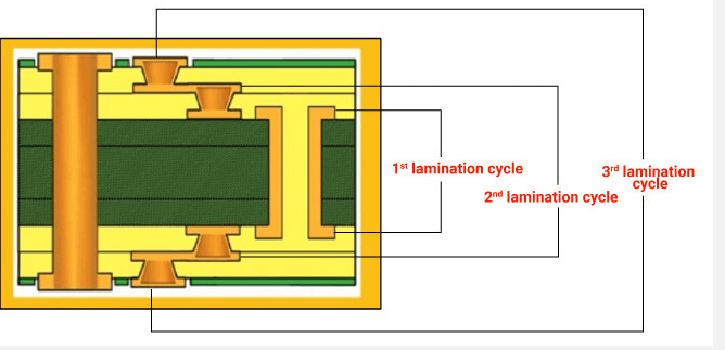
Traditional Circuit Board Sequential Lamination
Today, multi-layer PCBs are used most of the time. This type of board is smaller in size. The components also used when manufacturing make the product more compact in density. In short, multi-layer circuit boards make Taofang easy to manage and can be used flexibly.
At the same time, the paste design of the PCB is a single-layer circuit board, which requires some convenient manufacturing methods. With a full understanding of manufacturing capabilities, it will be easy to do this.
Sequential lamination is a common step in the PCB manufacturing process. The process is described as follows-
Sequential lamination has a high success rate on multi-layer boards. Especially in high-density electronics, it is more fruitful. This is the main function of maintaining high-signal messages such as communications.
Some Challenges that Sequential Lamination Must Face
The entire process of lamination is not so easy, and it seems that multiple challenges must be met in stages during its process. Like-
Restriction on the number of cycles
As mentioned earlier, in order to achieve good lamination results, more than two cycles are required. But this does not mean that it can be completed at any time you wish. Cycling must be limited to two to four times to prevent poor assembly.
Aspect Ratio
For drilling equipment, the other factor that must be considered is the aspect ratio. The aspect ratio is a measure of the depth in terms of the diameter of the drill hole.
Depending on the type of equipment used in the via (beam drill or drill press), the ratio varies and is calculated accordingly. The aspect ratio limits the layers used for different calculations in multi-layer circuits.
Drill alignment if Garber files are used
Gerber is a commonly used 2D file in PCB design. Designers like Garber files because of its software generation capabilities in PCB circuits.
But there are still some problems in the lamination process of Gerber files because there is a high probability of making mistakes while manufacturing the board. This results in misalignment of the circuit. This type of error increases the overall cost and turnaround time of the circuit.
Cost
Sequential lamination is a spontaneous build process that takes several days to build the required board. Therefore, the more time it takes to develop the circuit, the more expenses that come with it.
Despite all these limitations, it is one of the best manufacturing processes in PCB circuit boards. This is very useful because it minimizes the circuit layers and can maintain the temperature as the environment changes. Not only that, it also reduces the weight of the copper layer. Sequential lamination reduces the need for buried or blind vias, which is also one of the advantages of this lamination.
Therefore, if the disadvantages of this lamination can be ignored, it will be a great boon for PCB technology.
Trends in Sequential Lamination:
By using sequential lamination, the number of layers is significantly reduced.
Making PCBs makes it easy to handle.
The structure of the circuit board is simplified.
Techniques for Sequential Lamination PCB:
Mentioned above are some of the disadvantages of lamination technology. Now, in this passage, we discuss the techniques that must be used in order to achieve the best sequential lamination results.
The reason for all these deformations is the number of layers used in PCBs. A large number of layers reduces the potential of PCBs. Therefore, if the number of layers used is reduced, it will be a reasonable way to solve these problems.
In order to minimize the number of layers, some embedded elements can be put into the layers. With this method, only a few layers are required in addition to the top and bottom layers.
The components used in the circuit board are properly aligned and each component is connected together. Passive components need to be used more to eliminate the defect. Active components are used to try to embed them between the layers of the circuit.
Another solution is to use 3D equipment instead of 2D. The more advanced technology of 3D helps to deal with the consequences of lamination.
Turnkey PCB assembly is an incredible remedy to solve all problems. Turnkey PCB assembly will solve all problems with its organized management.
From manufacturing, maintenance, stacking to delivery, Taofang’s advanced technology has been corrected. And turnkey printed circuit boards are also very reliable and safe. You can trust its work efficiency.
The promise of sequential lamination is very simple. It provides PCB multi-layer stacking, providing security for your valuable files. PCB lamination technology will be a good choice for circuit design. Therefore, if you want to assemble your circuit with the latest, ready-to-use modern PCB, you must use sequential lamination PCB.