Mentor Graphics Application PCB Design Reuse
Introduction
As PCB boards tend to be miniaturized, multi-layered and complex. Especially for high-speed printed boards, it takes a long time of repeated debugging before they can be finalized. If there is a finalized design (A), and now a design (B) with the same or similar circuit as it is required, the traditional design process is as follows:
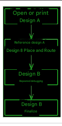
Figure 1: Traditional Design Flowchart
From this flowchart, it can be seen that design B adopts the idea of design A and manually repeats the design process of design A.
Implementation method
As a large-scale EDA software, Board Station not only has a wide range of applications and powerful functions, but also all design files are saved in ASCII code format, allowing users to modify design data, providing a basis for the reuse of PCB design.
Open a PCB design, and its main file structure is as follows:
Schematic path is the schematic data file; Design_geom path is the physical device (Geometry) data file; Pcb path is the printed board data file, among which comps is the component data file, including device reference (Reference), logic symbol (Symbol), corresponding physical device (Geometry), location on the printed board (Board_location) and properties (Properties) and other information; Nets is the netlist data file; traces is the printed board connection data file, including netlist name (NET), connection width, physical layer, start and end point coordinates and other information. The files under a design are far more than this, but other files can be automatically generated or derived by Board Station.
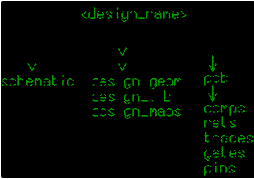
Figure 2: Main file structure of Board Station software
Board Station includes five modules: Design Architect, Librarian, Package, Layout, and Fablink. Assume that design A is the design currently in progress and design B is the design that needs to be reused. First, open Design A in the Design Architect module and copy the schematic diagram of the reused part of Design B to Design A; then, copy the physical device (Geometry) of the reused part of Design B from the Design_geom path of Design B to the Design_geom path of Design A; third, copy the component data of the reused part of Design B from the comps file of Design B to the comps file of Design A; fourth, refer to the netlist (NET) data of the reused part in the Nets file of Design B and modify the corresponding part in the Nets file of Design A; finally, copy the traces file of Design B to the pcb path of Design A to realize PCB design reuse.
Application example
The following takes Design A as the ongoing design and Design B as the reused design to illustrate the implementation method of PCB design reuse.
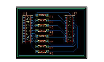
Figure 3: PCB diagram and schematic diagram of Design B
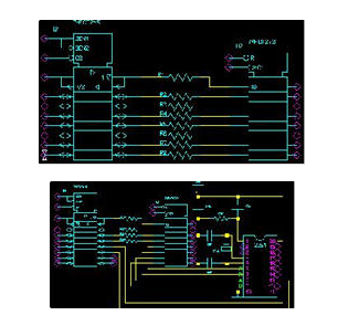
Figure 4: Schematic diagram of Design A
Follow the steps below:
- Draw the schematic diagram of Design A according to Figure 4 in the Design Architect module and store it.
- Enter the Librarian module of design A, create physical devices (Geometry) and mapping files, etc.
If the physical device (Geometry) corresponding to any of the devices U1, U2, R1, R2, R3, and R4 in Figure 4 is different from the physical device (Geometry) of the corresponding device in Figure 3, copy the corresponding physical device (Geometry) under the Design_geom path of design B to the Design_geom path of design A. That is, the physical devices (Geometry) of devices U1, U2, R1, R2, R3, and R4 in design A and design B must be the same.
In order to ensure that the physical devices (Geometry) corresponding to the devices U1, U2, R1, R2, R3, and R4 in Figure 4 are in the same position on the printed boards of design A and design B, copy the printed board Geometry (Board) of design B from the Design_geom path of design B to the Design_geom path of design A, and then modify it in the Librarian module. After completing all functions, save and exit. - Enter the Package module of design A, establish the correspondence between the logical symbol (Symbol) and the physical device (Geometry), and after completing all functions, save and exit.
- Modify the comps file of design A.
In any module of the Board Station software, use the drop-down menu MGC–>Notepad–>Open–>Edit…
Open the comps file of design B, select and copy (Copy) the lines related to devices U1, U2, R1, R2, R3, and R4.
Open the comps file of design A, select and delete (Delete) the lines related to devices U1, U2, R1, R2, R3, and R4, and then paste (Paste).
That is, the contents of devices U1, U2, R1, R2, R3, and R4 in the comps files of design A and design B must be the same. 5. Modify the Nets file of design A.
BOARD STATION NETS FILE FORMAT 1.0
Application: PACKAGE v8.6_4.1 Thu May 20 11:26:46 PDT 1999
date : Saturday October 14, 2000; 04:30:40
NET ‘/N$2’ U3-4 U7-2
NET ‘/N$3’ U3-5 U6-2
NET ‘/N$4’ U3-1 U8-1 U4-2
NET ‘/N$7’ U2-14 U3-7
NET ‘/N$8’ U2-13 U3-6
NET ‘/N$9’ U2-18 U3-9
NET ‘/N$10’ U2-17 U3-8
NET ‘/N$29’ R1-2 U2-3
NET ‘/N$30’ R2-2 U2-4
NET ‘/N$40’ R3-2 U2-7
NET ‘/N$41’ U2-8 R4-2
NET ‘/N$45’ U1-14 U3-11
NET ‘/N$46’ U1-13 U3-13
NET ‘/N$47’ R1-1 U1-18
NET ‘/N$48’ R2-1 U1-17
NET ‘/N$49’ R3-1 U1-16
NET ‘/N$50’ U1-15 R4-1
NET ‘GROUND’ U5-2 U3-10 U7-1 U8-2 U6-1 U1-10 U2-10
NET ‘VCC’ U5-1 U3-20 U4-1 U1-20 U2-20 (Table 1: Nets file for design A)
BOARD STATION NETS FILE FORMAT 1.0
Application : PACKAGE v8.6_4.1 Thu May 20 11:26:46 PDT 1999
date : Monday November 20, 2000; 12:52:50
NET ‘/N$9’ R1-1 U1-18
NET ‘/N$23’ R3-2 U2-7
NET ‘/N$25’ R5-2 U2-13
NET ‘/N$27’ R7-2 U2-17
NET ‘/N$230’ R2-2 U2-4
NET ‘/N$231’ R4-2 U2-8
NET ‘/N$232’ R6-2 U2-14
NET ‘/N$233’ R8-2 U2-18
NET ‘/N$234’ R1-2 U2-3
NET ‘/N$235’ R2-1 U1-17
NET ‘/N$236’ R3-1 U1-16
NET ‘/N$237’ R4-1 U1-15
NET ‘/N$238’ R5-1 U1-14
NET ‘/N$239’ R6-1 U1-13
NET ‘/N$240’ R7-1 U1-12
NET ‘/N$241’ R8-1 U1-11
NET ‘GROUND’ U1-10 U2-10
NET ‘VCC’ U1-20 U2-20 (Table 2: Nets file of design B)
In any module of the Board Station software, use the drop-down menu MGC–>Notepad–>Open–>Edit…
Reference Table 2 to modify Table 1, that is, change the NET names of the same pins in the Nets file of design A and the Nets file of design B to be the same. For example: if the first line in the Nets file of design B is NET ‘/N$9’ R1-1 U1-18, then change the corresponding line NET ‘/N$47’ R1-1 U1-18 in the Nets file of design A to NET ‘/N$9’ R1-1 U1-18.
If the modified NET name in the Nets file of design A is the same as the original NET name, modify the original NET name.
BOARD STATION NETS FILE FORMAT 1.0
Application: PACKAGE v8.6_4.1 Thu May 20 11:26:46 PDT 1999
# date: Saturday October 14, 2000; 04:30:40
#
NET ‘/N$2’ U3-4 U7-2
NET ‘/N$3’ U3-5 U6-2
NET ‘/N$4’ U3-1 U8-1 U4-2
NET ‘/N$7’ U2-14 U3-7
NET ‘/N$8’ U2-13 U3-6
NET ‘/N$99’ U2-18 U3-9
NET ‘/N$10’ U2-17 U3-8
NET ‘/N$234’ R1-2 U2-3
NET ‘/N$230’ R2-2 U2-4
NET ‘/N$23’ R3-2 U2-7
NET ‘/N$231’ U2-8 R4-2
NET ‘/N$45’ U1-14 U3-11
NET ‘/N$46’ U1-13 U3-13
NET ‘/N$9’ R1-1 U1-18
NET ‘/N$235’ R2-1 U1-17
NET ‘/N$236’ R3-1 U1-16
NET ‘/N$237’ U1-15 R4-1
NET ‘GROUND’ U5-2 U3-10 U7-1 U8-2 U6-1 U1-10 U2-10
NET ‘VCC’ U5-1 U3-20 U4-1 U1-20 U2-20 (Table 3: Nets file of modified design A)
6.Copy the traces file of design B to design A
Open the drop-down menu MGC–>Design Management–>Copy Object…
Select in the Options… option:
- Update All References
- Overwrite All File Conflicts
- Create Destination
In this way, all the connections related to design A on the PCB in design B are copied to the PCB of design A.
- Enter the Layout module of design A, and the interface shown in Figure 5 will appear without any operation.
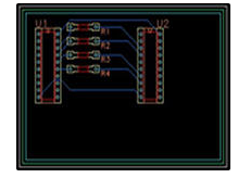
Figure 5: Part of the PCB diagram reused in design B
So far, the PCB design reuse from design B to design A is completed.
Conclusion
As a large-scale EDA software, Board Station software can not only perform board-level design, but also system-level and gate-level design, as well as schematic simulation, board-level simulation, etc. This article only discusses some techniques in PCB design, hoping to provide a reference for system-level, gate-level and other design reuse and simulation reuse.