Metal Core PCB in Power Electronics: IGBT, MOSFET, and Rectifier Applications
Power electronics design demands efficient thermal management alongside electrical performance. Metal Core PCBs (MCPCBs) solve this challenge by integrating a metal substrate directly into the board structure, providing superior heat dissipation for high-power components like IGBTs, MOSFETs, and rectifier modules. This guide explains how to design MCPCBs for power electronics applications, covering material selection, thermal design rules, and DFM considerations that impact both performance and manufacturability.
Table of Contents
- What Makes Metal Core PCB Critical for Power Electronics
- MCPCB Structure and Thermal Performance Parameters
- Design Rules for IGBT, MOSFET, and Rectifier Mounting
- Thermal Resistance Calculation and Material Selection
- DFM Considerations for MCPCB Manufacturing
- Application-Specific Design Guidelines
- FAQ
- Conclusion and Design Recommendations
1. What Makes Metal Core PCB Critical for Power Electronics
Standard FR4 PCBs have thermal conductivity around 0.3 W/m·K, which creates a thermal bottleneck in power electronics where IGBTs and MOSFETs can dissipate 50–200W per device. Metal Core PCBs use an aluminum or copper base layer with thermal conductivity of 140–400 W/m·K, dramatically improving heat transfer from semiconductor junction to heatsink.
The critical advantage in power electronics is maintaining junction temperature within safe operating limits. For example, an IGBT rated for 175°C junction temperature can experience thermal runaway if the PCB cannot conduct heat away fast enough. MCPCBs reduce the thermal resistance path by 60–80% compared to FR4, directly extending component lifespan and enabling higher power density designs.
Three key reasons power electronics engineers choose MCPCBs:
Thermal management: Direct thermal path from component to metal base eliminates reliance on thermal vias and copper planes. An MCPCB with 2 W/m·K dielectric can achieve junction-to-case thermal resistance below 1°C/W for TO-247 packages.
Mechanical stability: Aluminum base provides rigidity and CTE matching closer to semiconductor packages than FR4, reducing thermal cycling stress on solder joints. This matters in automotive and industrial applications with -40°C to +125°C ambient temperature swings.
EMI shielding: Grounded metal base layer acts as an effective shield for high-frequency switching noise generated by fast-switching MOSFETs and IGBTs, reducing radiated emissions without additional shielding layers.
2. MCPCB Structure and Thermal Performance Parameters
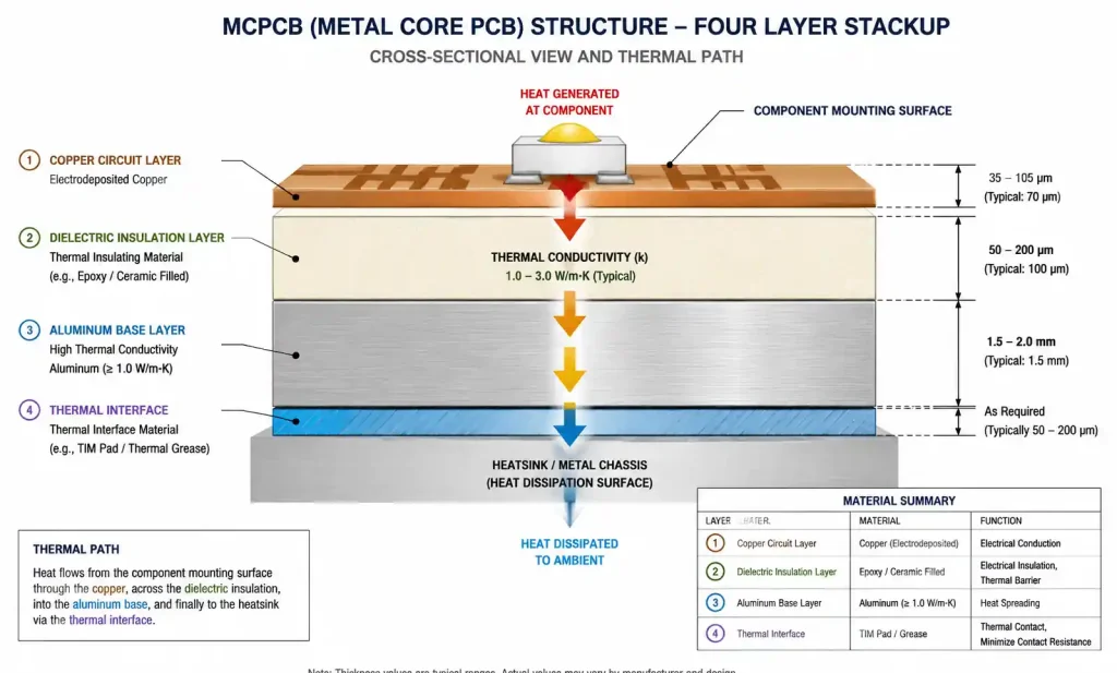
A typical Metal Core PCB consists of four layers from top to bottom: copper circuit layer, dielectric insulation layer, metal base layer, and optional thermal interface coating. Understanding each layer’s thermal contribution is essential for accurate thermal design.
Core Layer Structure
The copper circuit layer (35–105 µm) carries electrical signals and power traces. Thicker copper improves current carrying capacity but adds thermal resistance between component and dielectric interface.
The dielectric insulation layer (50–200 µm) provides electrical isolation between copper circuit and grounded metal base while conducting heat vertically. This layer’s thermal conductivity is the primary design variable, ranging from 1 W/m·K for standard epoxy-based dielectrics to 4–6 W/m·K for advanced ceramic-filled polymers.
The metal base layer (1.0–3.0 mm) is typically aluminum alloy 5052 or 6061 for cost-effective designs, or copper for maximum thermal performance. Aluminum provides thermal conductivity of 140–200 W/m·K at lower cost and weight, while copper offers 380–400 W/m·K but increases material cost by 3–4×.
Thermal Performance Comparison
The table below compares thermal resistance for different MCPCB configurations mounting a TO-247 power package:
| MCPCB Configuration | Dielectric Thermal Conductivity | Dielectric Thickness | Base Material | Junction-to-Case Thermal Resistance | Typical Application |
|---|---|---|---|---|---|
| Standard MCPCB | 1.0 W/m·K | 100 µm | 1.5mm Aluminum | 1.2–1.5°C/W | LED drivers, low-power converters |
| High-performance MCPCB | 2.0 W/m·K | 75 µm | 1.5mm Aluminum | 0.8–1.0°C/W | Motor drives, IGBT modules |
| Premium MCPCB | 4.0 W/m·K | 50 µm | 2.0mm Aluminum | 0.5–0.7°C/W | EV inverters, high-power rectifiers |
| Copper base MCPCB | 3.0 W/m·K | 75 µm | 1.5mm Copper | 0.4–0.6°C/W | Aerospace, military power supplies |
Higher dielectric thermal conductivity and thinner dielectric layers reduce thermal resistance, but cost increases exponentially. For IGBT applications dissipating over 100W per device, target thermal resistance below 0.8°C/W. For MOSFET-based converters with 20–50W dissipation, standard 1–1.5°C/W configurations often suffice.
The dielectric breakdown voltage also constrains thickness selection. For 600V–1200V IGBT modules, maintain minimum 75 µm dielectric thickness to ensure 2.5kV breakdown voltage with safety margin. Testing per IPC-TM-650 method 2.5.6 verifies dielectric withstand voltage before production.
3. Design Rules for IGBT, MOSFET, and Rectifier Mounting
Power semiconductor mounting on MCPCBs requires attention to thermal, electrical, and mechanical design rules that differ from standard PCB design practices.
Copper Pad Design for Thermal Performance
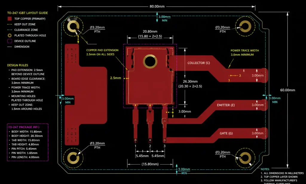
The copper pad directly under the power device must be sized to maximize thermal coupling while maintaining electrical isolation requirements. For TO-247, TO-220, and similar through-hole packages, the pad should extend 2–3 mm beyond the device mounting tab in all directions to ensure uniform heat spreading into the dielectric layer.
Avoid creating narrow copper traces immediately adjacent to high-power device pads. The trace acts as a thermal choke, creating hot spots. Instead, route power traces at least 5 mm away from the mounting pad edge, using wide traces (≥3 mm) for high current paths.
For surface-mount power packages like D²PAK, LFPAK, and PowerPAK, the thermal pad should match the datasheet recommended land pattern exactly. Deviating from the manufacturer’s recommendation can create voids during reflow, dramatically increasing thermal resistance.
Electrical Clearance and Creepage
Power electronics designs must meet safety clearance requirements between high-voltage nodes and the grounded metal base. For 600V systems, maintain minimum 2.5 mm clearance between any copper trace and the board edge where metal base is exposed. For 1200V systems, increase this to 4.0 mm.
The dielectric layer provides isolation between circuit copper and metal base, but traces near mounting holes or board edges can create partial discharge paths. Use keepout zones of 3 mm radius around all mounting holes that expose the metal base.
| Package Type | Recommended Pad Extension | Minimum Trace Width | Clearance to Board Edge | Typical Applications |
|---|---|---|---|---|
| TO-247 (3-pin) | 2.5 mm all sides | 3.0 mm (100A) | 3.0 mm (600V) | IGBT half-bridge, MOSFET H-bridge |
| TO-220 (3-pin) | 2.0 mm all sides | 2.5 mm (50A) | 2.5 mm (600V) | Flyback rectifiers, buck converters |
| D²PAK (SMD) | Match datasheet land | 2.0 mm (30A) | 2.5 mm (600V) | Synchronous rectifiers, low-side MOSFETs |
| IMS modules | 3.0 mm all sides | 5.0 mm (200A) | 4.0 mm (1200V) | Three-phase inverters, traction inverters |
For designs combining high-voltage IGBTs (600V–1200V) and low-voltage gate drive circuits (15–20V) on the same MCPCB, partition the layout with physical separation and guard traces connected to ground. This prevents high dV/dt switching transients from coupling into sensitive analog circuits.
Mounting Hole Placement and Mechanical Stress
Power devices generate clamping force during screw mounting that can crack the dielectric layer if holes are poorly positioned. Maintain minimum 5 mm distance between device mounting holes and board edge. For large IGBT modules with multiple mounting points, ensure hole positions match the device footprint with ±0.2 mm tolerance to prevent bending stress during installation.
Use plated through-holes for mounting holes to prevent metal base oxidation and improve grounding. The plating connects circuit ground to the metal base, providing a low-impedance return path for switching currents.
4. Thermal Resistance Calculation and Material Selection
Accurate thermal modeling determines whether your MCPCB design will maintain component junction temperature within rated limits under worst-case operating conditions.
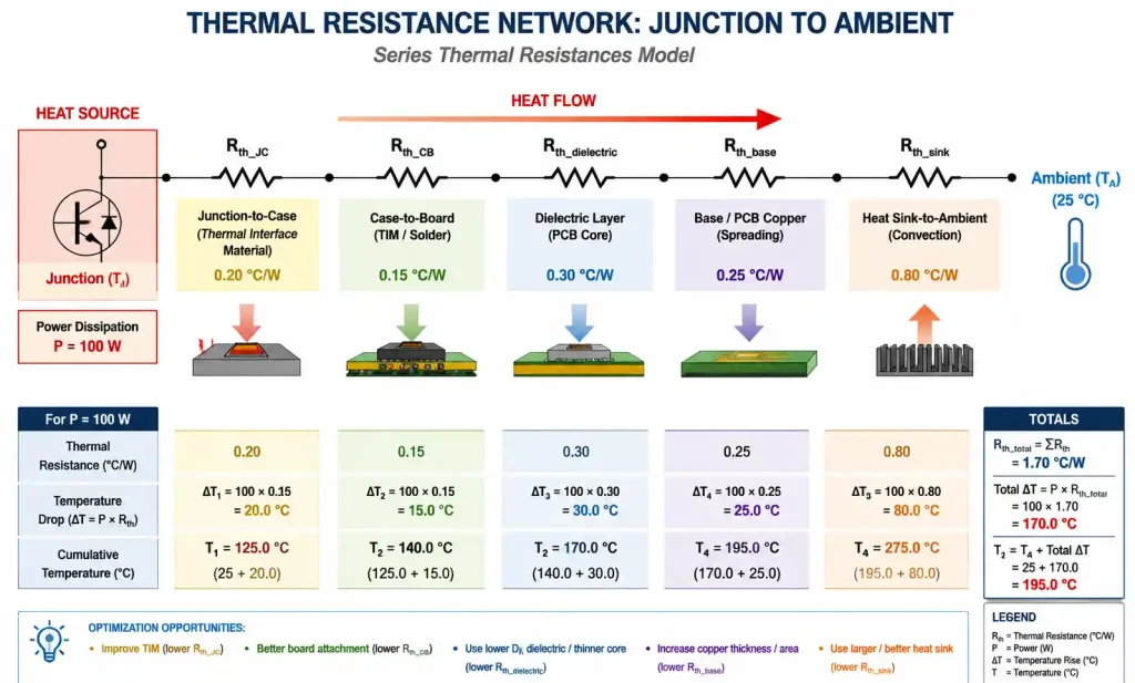
Thermal Resistance Path Analysis
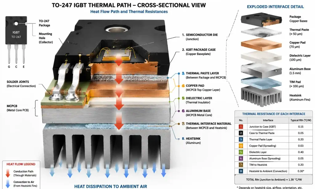
Total thermal resistance from semiconductor junction to ambient air consists of series resistances: junction-to-case (Rth_JC), case-to-board (Rth_CB), board dielectric (Rth_diel), metal base (Rth_base), and base-to-heatsink (Rth_sink).
The junction-to-case resistance is fixed by the semiconductor package design, typically 0.2–0.5°C/W for modern IGBT and MOSFET packages. This value appears in the component datasheet.
The case-to-board resistance depends on thermal interface material and mounting pressure. With thermal paste and 4 N·m torque, expect 0.1–0.2°C/W. Without thermal paste, this can increase to 0.5–1.0°C/W due to air gaps.
The dielectric layer resistance is calculated as: Rth_diel = t / (k × A), where t is dielectric thickness in meters, k is thermal conductivity in W/m·K, and A is copper pad area in m². For a TO-247 device with 150 mm² pad area, 75 µm dielectric at 2.0 W/m·K gives Rth_diel = 0.25°C/W.
The metal base resistance is typically negligible (< 0.05°C/W) due to high thermal conductivity and large cross-sectional area. The base-to-heatsink interface contributes 0.1–0.3°C/W depending on mounting surface finish and thermal interface material quality.
Material Selection Decision Tree
Choose dielectric thermal conductivity based on power dissipation per device and allowable temperature rise. For devices dissipating over 100W with strict junction temperature limits (< 150°C max), specify 3–4 W/m·K dielectric. For 30–100W dissipation with relaxed thermal requirements, 1.5–2.0 W/m·K provides adequate performance at lower cost.
Select base material thickness based on mechanical requirements and thermal mass needs. Thicker bases (2–3 mm) improve rigidity for large boards and provide thermal mass for transient power pulses, but increase weight. Standard 1.5 mm aluminum suits most applications.
| Power Dissipation per Device | Recommended Dielectric k | Recommended Thickness | Base Material | Estimated Cost Multiplier |
|---|---|---|---|---|
| < 30W (MOSFETs, small rectifiers) | 1.0–1.5 W/m·K | 100 µm | 1.5mm Aluminum | 1.0× baseline |
| 30–80W (medium power MOSFETs) | 1.5–2.0 W/m·K | 75–100 µm | 1.5mm Aluminum | 1.3–1.5× |
| 80–150W (IGBTs, high-current rectifiers) | 2.0–3.0 W/m·K | 50–75 µm | 1.5–2.0mm Aluminum | 1.8–2.2× |
| > 150W (EV inverters, traction drives) | 3.0–4.0 W/m·K | 50 µm | 2.0mm Aluminum or Copper | 2.5–4.0× |
These cost multipliers are relative to standard 1.0 W/m·K MCPCB. High-performance dielectrics require specialized manufacturing processes and materials, driving cost increases. Balance thermal performance against budget constraints by optimizing pad size and heatsink selection rather than always choosing premium dielectrics.
For applications with multiple power devices at different power levels on one board, zone the design. Place highest power devices over premium dielectric areas and lower power devices over standard dielectric regions to optimize cost. Some manufacturers offer multi-zone MCPCBs with different dielectric specifications in different board areas.
5. DFM Considerations for MCPCB Manufacturing
Metal Core PCB manufacturing differs from standard PCB processes, introducing specific design-for-manufacturability requirements that prevent yield loss and ensure reliable thermal performance.
Routing and Panelization Challenges
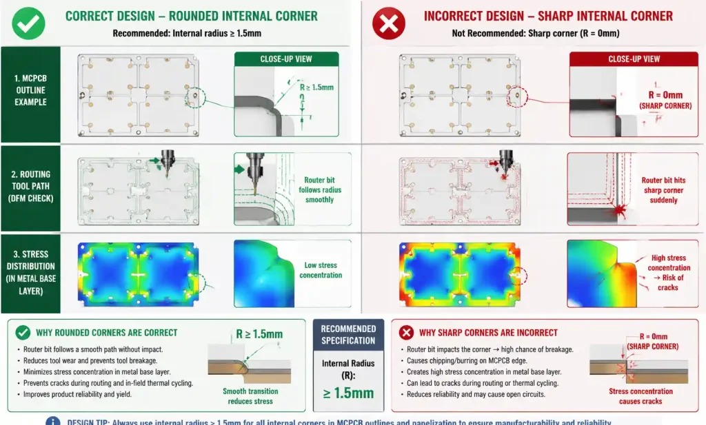
MCPCBs cannot be routed using standard CNC milling due to the metal base layer. Manufacturers use CNC routing with specialized bits or laser cutting for board outlines. Sharp internal corners (< 1 mm radius) cause tool breakage or stress concentrations. Design all internal corners with minimum 1.5 mm radius.
V-groove scoring is not possible with metal base PCBs. If panelization is required for assembly efficiency, use tab routing with 3–5 mm wide tabs between individual boards. Depaneling requires shearing or saw cutting rather than snap-apart methods.
Board thickness tolerance is ±0.1 mm for standard aluminum MCPCBs due to the metal base thickness variation. This impacts component standoff height for through-hole devices. Specify mounting hole counter-boring if precise component height is critical.
Drilling and Plating Requirements
Through-holes in MCPCBs must penetrate copper, dielectric, and metal base layers. Standard carbide drill bits wear rapidly on aluminum, requiring frequent replacement and increasing manufacturing cost. Holes smaller than 0.8 mm diameter are challenging to drill reliably in MCPCBs.
Plated through-holes in MCPCBs provide electrical connection and improved thermal transfer but require specialized plating processes. The metal base must be masked during electroplating to prevent short circuits. Non-plated holes are more cost-effective for mounting holes that only require mechanical function.
For power devices requiring electrical isolation from the metal base, use non-plated mounting holes with insulating bushings. This prevents accidental shorts if solder wicks into the hole during assembly.
DFM Checklist for MCPCB Power Electronics
The following checklist prevents common manufacturing issues specific to metal core boards:
| Design Element | DFM Requirement | Reason | Risk if Violated |
|---|---|---|---|
| Internal corner radius | ≥ 1.5 mm | Routing tool limitations | Board breakage, stress cracks |
| Minimum hole diameter | ≥ 0.8 mm | Drilling in metal base | Drill breakage, hole quality |
| Copper trace to board edge | ≥ 3.0 mm | Routing tolerance | Copper exposure, short to base |
| Minimum trace width | ≥ 0.3 mm (signal), ≥ 2.0 mm (power) | Etching process variation | Open circuits, insufficient current capacity |
| Solder mask clearance | ≥ 0.1 mm | Registration accuracy on metal base | Solder bridges, poor insulation |
| Component keepout from edge | ≥ 5.0 mm | Thermal stress, routing tolerance | Component damage during depaneling |
| Panel tab width | ≥ 3.0 mm | Depaneling strength | Board damage during separation |
Before submitting MCPCB designs to manufacturing, request a DFM review from your fabricator. Manufacturing capabilities vary significantly between MCPCB suppliers, particularly for high-performance dielectrics and tight tolerances. Early engagement prevents costly design iterations.
6. Application-Specific Design Guidelines
Different power electronics applications place distinct requirements on MCPCB design. Optimize your layout for the specific demands of your target application.
IGBT Half-Bridge and Three-Phase Inverters
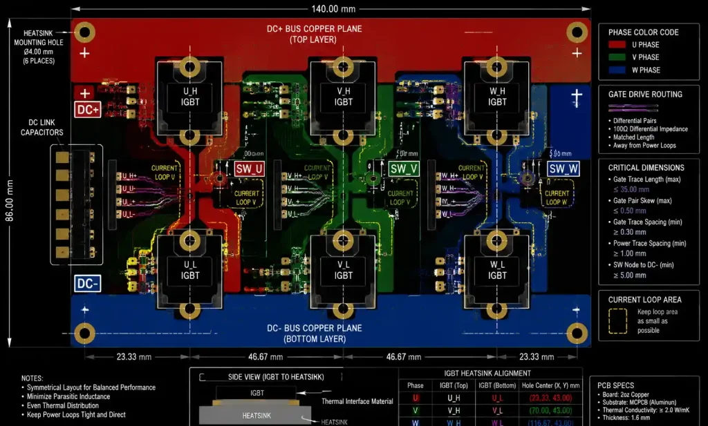
IGBT inverters for motor drives and EV traction systems require MCPCBs that handle high power dissipation (100–300W per IGBT), high voltage isolation (600–1200V), and low parasitic inductance for gate drive circuits.
Place high-side and low-side IGBTs on opposite sides of the DC bus copper plane to minimize loop inductance. This reduces voltage overshoot during turn-off, which can exceed IGBT voltage rating and cause failure. Target loop inductance below 20 nH for 600V applications.
Use separate copper pours for each IGBT’s collector and emitter connections, with wide traces (≥ 5 mm) for current paths rated at 100A or higher. Gate drive traces should be short (< 30 mm), narrow (0.5–1.0 mm), and routed as differential pairs to reject common-mode noise from high dV/dt switching.
Position gate drive components (gate resistors, diodes, capacitors) within 10 mm of IGBT gate and emitter pins. Longer trace lengths increase parasitic inductance, slowing gate drive response and increasing switching losses.
For three-phase inverters, arrange IGBTs in a linear or triangular pattern to balance thermal distribution. Avoid clustering all six IGBTs in one area, which creates a thermal hot spot exceeding the heat sink’s capacity to dissipate.
Synchronous Rectifier MOSFETs in DC-DC Converters
Synchronous buck and boost converters use low-voltage MOSFETs (20–60V) with very low Rds(on) (< 5 mΩ) to minimize conduction losses. Despite low voltage drop, these MOSFETs can dissipate 10–30W at 20A continuous current.
MCPCBs for synchronous rectifiers prioritize low thermal resistance over high voltage isolation. Standard 1.5–2.0 W/m·K dielectric with 100 µm thickness provides adequate performance while keeping cost reasonable for consumer electronics applications.
Place the high-side and low-side MOSFETs adjacent to each other with the switching node connection (SW) between them as short as possible. This minimizes the high-frequency loop containing input capacitors, MOSFETs, and output inductor. Loop area under 100 mm² reduces radiated EMI and improves efficiency by limiting ringing.
Use copper thicknesses of 70–105 µm (2–3 oz) for power traces handling over 10A continuous current. Standard 35 µm (1 oz) copper has excessive voltage drop and heating at high currents. Calculate trace width using IPC-2221 current capacity curves with 20°C temperature rise as maximum limit for MCPCB designs.
High-Frequency Rectifier Modules
Rectifier modules for AC-DC converters, welding power supplies, and motor drives combine multiple diodes or MOSFETs in parallel to handle 50–200A currents. MCPCBs enable compact module designs with integrated thermal management.
Parallel-connected rectifiers require careful attention to current sharing. Use symmetric copper trace layouts with equal trace lengths and widths from AC input to each device. Asymmetric layouts cause unequal current distribution, overloading some devices while under-utilizing others.
Add Kelvin sensing connections for output voltage measurement, routed separately from high-current power traces. This prevents voltage drop in power traces from affecting regulation accuracy, particularly important for precision power supplies maintaining ±1% output voltage tolerance.
For fast-recovery diodes in PFC (power factor correction) circuits switching at 65–100 kHz, minimize reverse recovery di/dt by placing small snubber capacitors (100–220 pF) directly across each diode with trace lengths under 5 mm. This reduces voltage ringing that generates EMI and stresses adjacent components.
7. FAQ
What is the thermal conductivity difference between aluminum and copper base MCPCBs?
Aluminum base MCPCBs offer 140–200 W/m·K thermal conductivity depending on alloy, while copper base provides 380–400 W/m·K. However, the dielectric layer (1–4 W/m·K) is the primary thermal bottleneck in most designs, making copper base only beneficial for extreme power density applications exceeding 200W per device. Copper base adds 3–4× material cost and 2× weight compared to aluminum. For most IGBT and MOSFET applications under 150W per device, aluminum base with optimized dielectric selection provides sufficient thermal performance at lower cost.
How do I calculate junction temperature for an IGBT on an MCPCB?
Junction temperature T_j = T_ambient + (P_dissipated × Σ Rth), where Σ Rth is the sum of all thermal resistances from junction to ambient. For example, with 100W dissipation, T_ambient = 50°C, Rth_JC = 0.35°C/W, Rth_CB = 0.15°C/W, Rth_dielectric = 0.50°C/W, and Rth_sink = 0.80°C/W: T_j = 50 + (100 × 1.80) = 230°C, which exceeds the IGBT’s 175°C maximum rating. You must improve thermal resistance or reduce power dissipation to maintain safe operation.
Can I mix high-voltage IGBTs and low-voltage control circuits on the same MCPCB?
Yes, but requires careful isolation design. Maintain minimum 3–4 mm clearance between high-voltage copper (600V–1200V) and low-voltage circuits (5–24V). Use guard traces connected to ground plane between high and low voltage zones. Route gate drive signals as differential pairs with ground shielding to reject dV/dt noise from IGBT switching. Verify clearance and creepage distances meet safety standards for your target application (UL, IEC, VDE). Consider using a slot routed through the copper and dielectric layers (but not the metal base) to provide physical separation between zones if board area permits.
What surface finish works best for MCPCB power electronics assembly?
ENIG (Electroless Nickel Immersion Gold) is the standard choice for MCPCBs due to flat surface for power package mounting, excellent solderability, and long shelf life. The nickel layer (3–6 µm) provides wear resistance for screw-mounted devices. HASL (Hot Air Solder Leveling) is lower cost but creates uneven surface topology that can increase thermal resistance at the package interface. For lead-free assembly of surface-mount power packages, ENIG ensures reliable solder joints without the thickness variation of HASL.
How thick should the dielectric layer be for 1200V IGBT modules?
For 1200V applications, specify minimum 75 µm dielectric thickness to achieve 2.5 kV breakdown voltage with safety factor. IPC standards require 2× rated voltage for breakdown testing. Thicker dielectrics (100–150 µm) provide additional safety margin but increase thermal resistance. For high-reliability applications (automotive, industrial), 100 µm at 2.0–3.0 W/m·K thermal conductivity balances electrical isolation and thermal performance. Always verify dielectric breakdown voltage with test reports from your MCPCB manufacturer before finalizing the design.
What is the typical lead time and MOQ for prototype MCPCB fabrication?
Prototype MCPCB lead times range from 5–10 business days for standard specifications (aluminum base, 1.0–2.0 W/m·K dielectric) to 15–20 days for high-performance builds (copper base, 3–4 W/m·K dielectric). Minimum order quantities vary from 5–10 pieces for prototypes to 50–100 pieces for production volumes. Express services can reduce lead time to 3–5 days with premium pricing. MCPCB costs are 3–8× higher than equivalent FR4 boards due to specialized materials and processing, so budget $50–200 per prototype board depending on size and specifications.
8. Conclusion and Design Recommendations
Metal Core PCBs deliver essential thermal management for power electronics applications where IGBTs, MOSFETs, and rectifiers operate at power levels exceeding standard FR4 capabilities. Success requires understanding the thermal resistance path, selecting appropriate dielectric materials, and following DFM rules specific to metal base board manufacturing.
For IGBT inverter designs dissipating over 100W per device, specify 2.0–3.0 W/m·K dielectric with 50–75 µm thickness and 1.5–2.0 mm aluminum base. This achieves junction-to-case thermal resistance below 1.0°C/W, maintaining junction temperature within safe limits even under worst-case conditions.
For MOSFET-based DC-DC converters with 30–80W dissipation, standard 1.5 W/m·K dielectric provides adequate performance while controlling costs. Focus design effort on minimizing parasitic inductance and optimizing copper trace widths for current carrying capacity.Before finalizing your MCPCB design, request a manufacturability review from your fabricator. Verify dielectric breakdown voltage test data, confirm thermal conductivity specifications, and review board outline tolerances. These steps prevent costly design iterations and ensure your power electronics design meets both electrical and thermal requirements.
For design support, download our MCPCB design checklist or submit your Gerber files for free DFM analysis. Our CAM engineering team specializes in power electronics MCPBs and can optimize your layout for manufacturability and thermal performance.