Methods and Techniques for PCB Sectioning: A Comprehensive Guide
Introduction
Printed Circuit Board (PCB) sectioning is an essential process in electronics manufacturing, failure analysis, quality control, and research & development. This technique allows engineers and technicians to examine the internal structure of PCBs, identify defects, verify layer alignment, and analyze material properties. With the increasing complexity of modern PCBs featuring high-density interconnects, microvias, and advanced materials, proper sectioning methods have become more critical than ever.
This article provides a comprehensive overview of various PCB sectioning methods and techniques, offering practical guidance for professionals working with PCB analysis. We’ll explore mechanical sectioning, chemical etching, laser cutting, and other specialized approaches, along with best practices for sample preparation, polishing, and microscopic examination.
1. Mechanical Sectioning Methods
1.1 Precision Saw Cutting
Precision saw cutting is one of the most common methods for PCB sectioning, offering a good balance between speed and accuracy. Diamond-coated or carbide blades are typically used for this purpose.
Key Techniques:
- Select appropriate blade grit size (typically 320-600 grit for PCBs)
- Maintain proper cutting speed (200-500 RPM depending on material)
- Use coolant to prevent overheating and material smearing
- Secure the PCB firmly to minimize vibration and chipping
- Make relief cuts for complex geometries
Advantages:
- Relatively fast process
- Suitable for most PCB materials
- Minimal chemical hazards
- Good for large sample preparation
Limitations:
- May cause mechanical stress in delicate structures
- Requires post-cutting polishing for smooth surfaces
- Potential for fiber pull-out in FR4 materials
1.2 Microtome Sectioning
Microtome sectioning provides extremely precise cuts for high-magnification analysis, particularly useful for multilayer PCBs with fine features.
Key Parameters:
- Knife angle: 5-15 degrees
- Section thickness: 10-100 μm
- Cutting speed: 0.5-2 mm/s
- Sample temperature: Room temperature or cryogenic for brittle materials
Best Practices:
- Embed samples in epoxy for support
- Use fresh, sharp blades for each critical sample
- Maintain consistent cutting parameters
- Clean samples between cuts to prevent contamination
2. Chemical Sectioning Techniques
2.1 Chemical Etching
Chemical etching selectively removes material to reveal internal structures without mechanical stress.
Common Etchants:
- Ferric chloride (FeCl₃) for copper examination
- Ammonium persulfate for clean copper revelation
- Sodium hydroxide (NaOH) for polymer layers
- Hydrofluoric acid (HF) for glass fiber inspection (with extreme caution)
Process Control:
- Temperature: 30-50°C typically
- Concentration: 10-40% depending on material
- Time: 30 seconds to several minutes
- Agitation: Improves etch uniformity
Safety Considerations:
- Always use proper PPE (gloves, goggles, ventilation)
- Neutralize and properly dispose of chemicals
- Work in fume hoods for volatile chemicals
2.2 Plasma Etching
Plasma etching offers anisotropic removal with excellent control for delicate structures.
Parameters to Control:
- Gas composition (CF₄, O₂, Ar mixtures)
- RF power (50-500W)
- Pressure (10-500 mTorr)
- Etch time (minutes to hours)
Applications:
- High aspect ratio via inspection
- Delicate IC package analysis
- Polymer layer characterization
3. Advanced Sectioning Methods
3.1 Focused Ion Beam (FIB) Sectioning
FIB provides nanometer-scale precision for cutting and imaging simultaneously.
Key Features:
- Gallium ion beam for material removal
- Electron beam for imaging
- Gas injection for enhanced etching or deposition
- Site-specific capability
Typical Applications:
- Failure analysis of individual vias or traces
- Cross-sectioning of microvias
- IC package inspection
- 3D tomography reconstruction
3.2 Laser Microsectioning
Laser systems offer contactless cutting with minimal mechanical stress.
Laser Types:
- UV lasers (355 nm) for precise cuts
- IR lasers for faster bulk removal
- Femtosecond lasers for minimal heat-affected zones
Optimization Parameters:
- Pulse energy (μJ to mJ range)
- Repetition rate (1-100 kHz)
- Scan speed (mm/s)
- Number of passes
- Assist gas (air, N₂, or inert gases)
4. Sample Preparation Techniques
4.1 Mounting and Embedding
Proper sample support is crucial for successful sectioning.
Options:
- Cold mounting resins (fast curing)
- Hot mounting compounds (better for hard materials)
- Transparent epoxy for edge retention
- Conductive coatings for electron microscopy
Techniques:
- Vacuum impregnation for porous materials
- Gradient curing for stress reduction
- Alignment fixtures for specific orientations
4.2 Grinding and Polishing
Post-sectioning preparation determines observation quality.
Progressive Steps:
- Coarse grinding (180-400 grit)
- Medium grinding (600-1200 grit)
- Fine grinding (2000-4000 grit)
- Diamond polishing (1-9 μm)
- Final polishing (0.05 μm alumina or silica)
Critical Factors:
- Consistent pressure (5-15 N typically)
- Proper lubrication/cooling
- Clean between steps
- Direction changes between grades
- Time control for soft materials
5. Imaging and Analysis
5.1 Optical Microscopy
Standard method for quick examination.
Enhancement Techniques:
- Differential interference contrast (DIC)
- Darkfield illumination
- Polarized light for crystalline materials
- High dynamic range imaging
5.2 Scanning Electron Microscopy (SEM)
Provides superior resolution and depth of field.
Preparation Requirements:
- Conductive coating (Au, Pd, or C)
- Proper grounding
- Optimal working distance
- Appropriate detector selection (SE, BSE)
5.3 3D Reconstruction
Advanced analysis through serial sectioning.
Methods:
- Mechanical serial polishing
- FIB-SEM tomography
- X-ray computed tomography
- Confocal microscopy
6. Specialized Sectioning Applications
6.1 High-Frequency PCB Analysis
Special considerations for RF materials:
- Low-damage cutting to preserve dielectric properties
- Careful handling of fragile ceramic-filled PTFE
- Special etchants for exotic substrates
6.2 Flexible Circuit Inspection
Unique challenges:
- Support during cutting
- Minimizing deformation
- Handling thin polyimide layers
- Adhesive layer examination
6.3 HDI Microvia Analysis
Critical parameters:
- Precise alignment for microvia chains
- Minimal smearing for laser-drilled vias
- Copper plating quality assessment
- Resin fill inspection
7. Best Practices and Troubleshooting
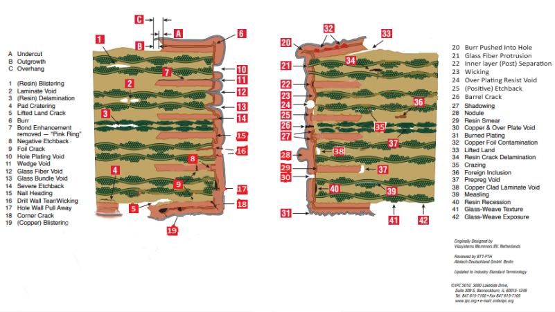
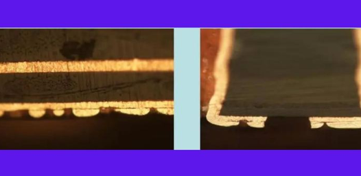
7.1 Common Artifacts and Solutions
- Smearing: Use sharper tools, lower force, or chemical polishing
- Delamination: Adjust embedding process, use vacuum impregnation
- Edge rounding: Optimize mounting hardness match
- Fiber pull-out: Consider chemical etching or plasma methods
- Heat damage: Reduce cutting speed, improve cooling
7.2 Measurement Accuracy
- Calibrate microscopes regularly
- Account for magnification distortions
- Use stage micrometers for verification
- Consider tilt compensation for angled features
7.3 Documentation Standards
- Consistent lighting conditions
- Scale bars in all images
- Orientation indicators
- Complete process documentation
- Comparison with known good samples
Conclusion
PCB sectioning is both an art and a science, requiring careful consideration of the board’s materials, structures, and analysis requirements. The choice between mechanical, chemical, or advanced sectioning methods depends on multiple factors including required precision, sample size, available equipment, and the specific features being examined.
By understanding the various techniques and their appropriate applications, engineers and technicians can select the most suitable approach for their specific needs. Proper sample preparation, careful execution of the sectioning process, and appropriate imaging techniques all contribute to obtaining meaningful results that can drive design improvements, process optimizations, and failure analysis conclusions.
As PCB technology continues to advance with finer features and more complex architectures, sectioning methods must similarly evolve. Staying informed about the latest techniques and equipment developments ensures that professionals can meet the growing challenges of PCB analysis in an increasingly miniaturized electronics industry.