
Optimizing PCB Layout for Synchronous Buck Converters
Introduction
Synchronous buck converters are widely used in modern power electronics due to their high efficiency, compact size, and ability to step down voltage efficiently. However, achieving optimal performance requires careful PCB (Printed Circuit Board) layout design. Poor layout practices can lead to increased electromagnetic interference (EMI), voltage spikes, excessive power losses, and even converter instability.
This article explores key strategies for optimizing the PCB layout of synchronous buck converters, focusing on minimizing parasitic elements, improving thermal management, and ensuring signal integrity.
1. Understanding the Critical Current Paths
A synchronous buck converter consists of high-frequency switching components, including a high-side MOSFET, low-side MOSFET (or synchronous rectifier), inductor, input/output capacitors, and a control IC. The current flows through different paths depending on the switching state:
- High-side FET ON: Current flows from the input capacitor through the high-side FET to the inductor and load.
- Low-side FET ON: Current circulates from ground through the low-side FET and inductor to the load.
These switching currents generate high di/dt (rate of current change) and dv/dt (rate of voltage change), making the PCB layout crucial for minimizing parasitic inductance and resistance.
Key Current Loops to Optimize:
- Power Loop (High-current path): Includes input capacitor → high-side FET → inductor → output capacitor → load.
- Switching Loop: High-side FET → low-side FET → ground.
- Gate Drive Loop: Controller → gate driver → MOSFET gates → return path.
Minimizing loop areas reduces parasitic inductance, which can cause voltage spikes and ringing.
2. Component Placement Strategies
2.1. Input Capacitor Placement
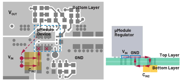
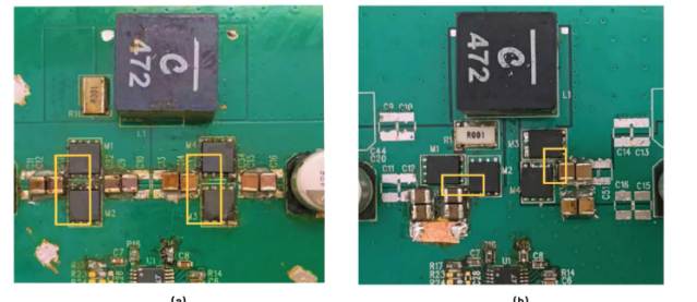
The input capacitors must be placed as close as possible to the drain of the high-side FET and the source of the low-side FET. This minimizes the high-frequency current loop and reduces parasitic inductance, which can cause voltage overshoot and EMI.
- Use multiple small ceramic capacitors in parallel to reduce equivalent series inductance (ESL).
- Place bulk capacitors (e.g., electrolytic) near the ceramic capacitors to handle lower-frequency ripple.
2.2. MOSFET Placement
The high-side and low-side MOSFETs should be placed adjacent to each other with minimal trace length between them.
- Use a copper pour or wide traces to reduce resistance and inductance.
- Ensure proper thermal vias under MOSFETs to dissipate heat efficiently.
2.3. Inductor Placement
The inductor should be positioned close to the switching node (connection between MOSFETs and inductor) to minimize high-frequency noise radiation.
- Avoid routing sensitive signals near the inductor to prevent magnetic coupling.
2.4. Output Capacitor Placement
Output capacitors should be placed near the load to minimize impedance and improve transient response.
- Use a combination of ceramic and bulk capacitors for optimal filtering.
3. PCB Layer Stackup Considerations
A well-designed layer stackup improves power integrity and reduces EMI.
Recommended Stackup for Buck Converters:
- Top Layer: High-current power traces, MOSFETs, and inductor.
- Inner Layer 1: Ground plane (critical for return currents).
- Inner Layer 2: Power plane (if needed for input/output distribution).
- Bottom Layer: Control signals, feedback traces, and gate drive circuits.
Key Practices:
- Use a solid ground plane to provide a low-impedance return path.
- Avoid splitting ground planes, which can increase loop inductance.
- Route high-frequency signals over a continuous ground plane.
4. Minimizing Parasitic Elements
4.1. Reducing Parasitic Inductance
- Keep high-current traces short and wide.
- Use multiple vias in parallel for high-current paths.
- Avoid sharp corners in traces (use 45° or curved bends).
4.2. Reducing Parasitic Capacitance
- Separate high dv/dt nodes (e.g., switching node) from sensitive traces.
- Use guard rings or ground shielding for noise-prone signals.
5. Thermal Management
Synchronous buck converters dissipate heat primarily through MOSFETs and inductors.
Best Practices:
- Use thermal vias under MOSFETs to transfer heat to inner or bottom layers.
- Increase copper area for power components to improve heat dissipation.
- Consider using exposed pads (ePAD) for power ICs and MOSFETs.
6. Signal Integrity and Noise Reduction
6.1. Feedback Trace Routing
The feedback (voltage sense) network is critical for regulation accuracy.
- Route feedback traces away from high-noise areas (inductor, switching nodes).
- Use a Kelvin connection for precise voltage sensing.
- Keep feedback traces short and close to the ground plane.
6.2. Gate Drive Routing
- Keep gate drive traces short to minimize inductance, which can slow down switching and increase losses.
- Use a dedicated ground return path for gate drivers.
6.3. Avoiding Ground Noise
- Separate power ground (PGND) and signal ground (SGND) if necessary, but tie them at a single point near the IC.
- Avoid ground loops that can introduce noise.
7. EMI Mitigation Techniques
High-frequency switching generates EMI, which can affect nearby circuits.
Key Methods:
- Use a Faraday shield (copper pour) around the switching node.
- Implement proper filtering on input and output lines.
- Use snubber circuits to dampen ringing.
8. Design Verification and Testing
After layout, perform simulations and physical tests:
- Use a thermal camera to identify hot spots.
- Measure switching waveforms with an oscilloscope to check for excessive ringing.
- Conduct EMI testing to ensure compliance with standards.
Conclusion
Optimizing the PCB layout for synchronous buck converters is essential for achieving high efficiency, low noise, and reliable operation. By minimizing parasitic elements, optimizing component placement, and implementing proper grounding and thermal management, designers can enhance performance and reduce EMI. Careful attention to detail during layout ensures that the converter operates as intended, delivering stable and efficient power conversion.
Following these guidelines will help engineers avoid common pitfalls and achieve a robust, high-performance buck converter design.