PCB assembly equipment
What is a PCB assembler?
Printed circuit board assembly is the process of connecting the electronic components with the wirings of printed circuit boards. The traces or conductive pathways engraved in the laminated copper sheets of PCBs are used within a non-conductive substrate in order to form the assembly
when a large number of PCBs are required, the components aren’t soldered by hand. Instead, manufacturers use professional assembly equipment to manufacture the PCBs.
These equipment falls into two broad categories, production and inspection equipment
PCBA production equipment
In the assembly of these miniature electronic brains, there are four surface mount technology assemblies (SMT). These follow the reflow method, and consist of:
Automatic solder paste printer
The first step in assembling PCBs is to apply a solder paste onto the board. This is a gray-colored paste made from tiny particles of various metal alloys. Usually, this consists of tin, lead, and silver.
It functions as a type of glue that can hold the completed board together. Without this paste, components wouldn’t stick.
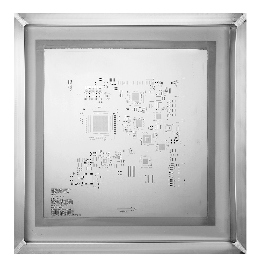
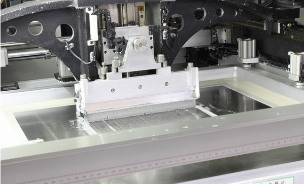
Before the paste can be applied, a stencil is placed on top of the board. This PCB stencil is a thin stainless steel sheet with small laser-cut holes. Then the solder paste is applied onto the board where the components are going to go.
The first significant piece of assembly equipment is the Solder Paste Printing Machine. This machine holds the PCB locked in place in the automated paste printer. Then, using proper amounts, a squeegee applies solder paste on the pads.
Next, a blade drags across the stencil and spreads the solder paste evenly in the holes, so only the areas of later contact get a layer of the glue. The stencil is removed by the machine after.
If all went well, the solder paste should now be where the components will be placed later.
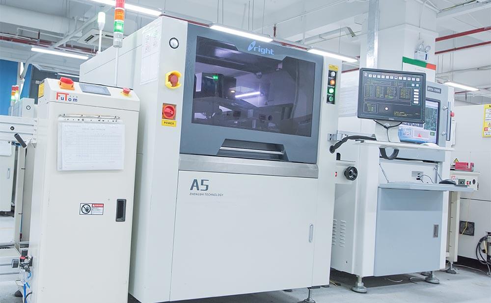
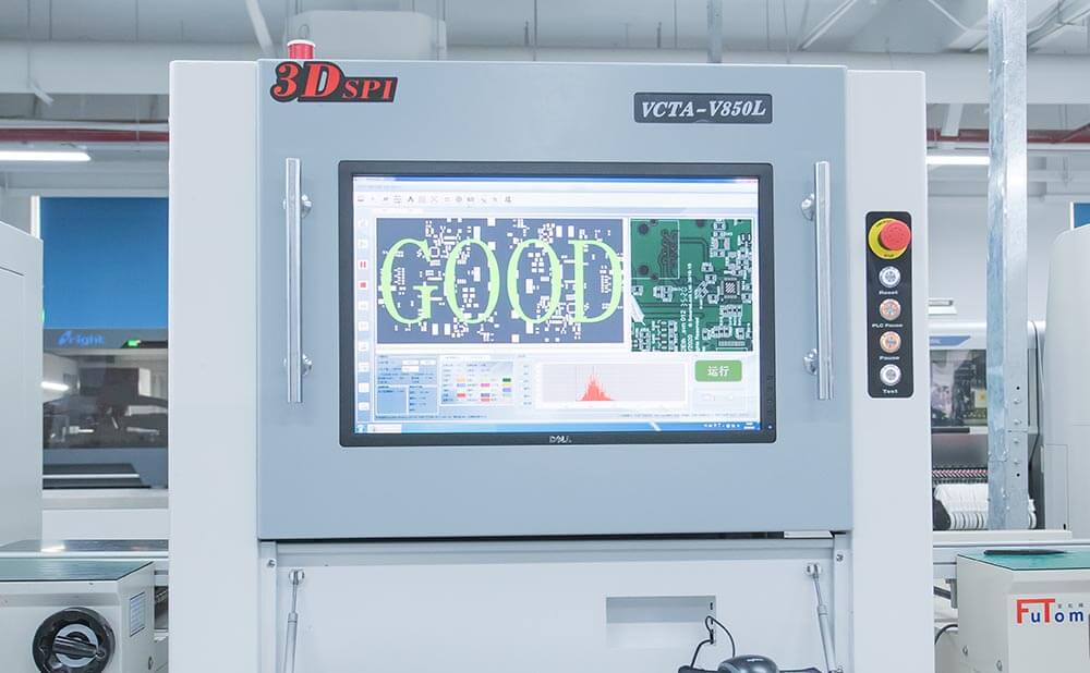
3D SPI (Solder Paste Inspection online)
SMD soldering issues are often traced to cheap solder paste printing. Any mistakes at this step can mean that the assembly overall is not as reliable or robust as it should be.
Therefore, the next step is to inspect the solder paste is appropriately printed onto the board using an SPI machine.
The SPI machine uses cameras to capture 3D images and evaluate the solder paste through solder volume, alignment, and height. It can also identify unsuitable sizes and imperfections so manufacturers can correct them.
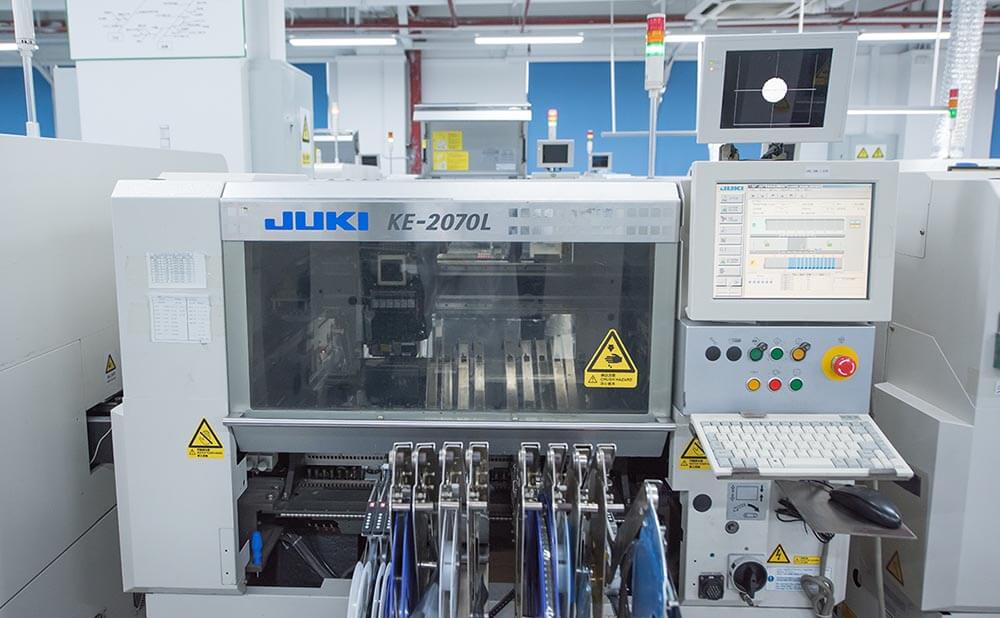
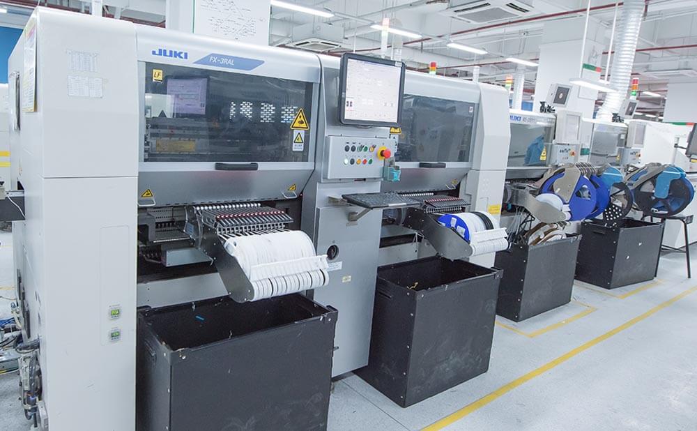
Automatic SMT machine
After the solder paste has been applied to a board, the PCBA process moves onto the pick-and-place SMD assembly machines. The machine suctions up SMT components and places them accurately on top of the solder paste in the pre-programmed positions.These robots can do this at a rate of 20,000 parts an hour.
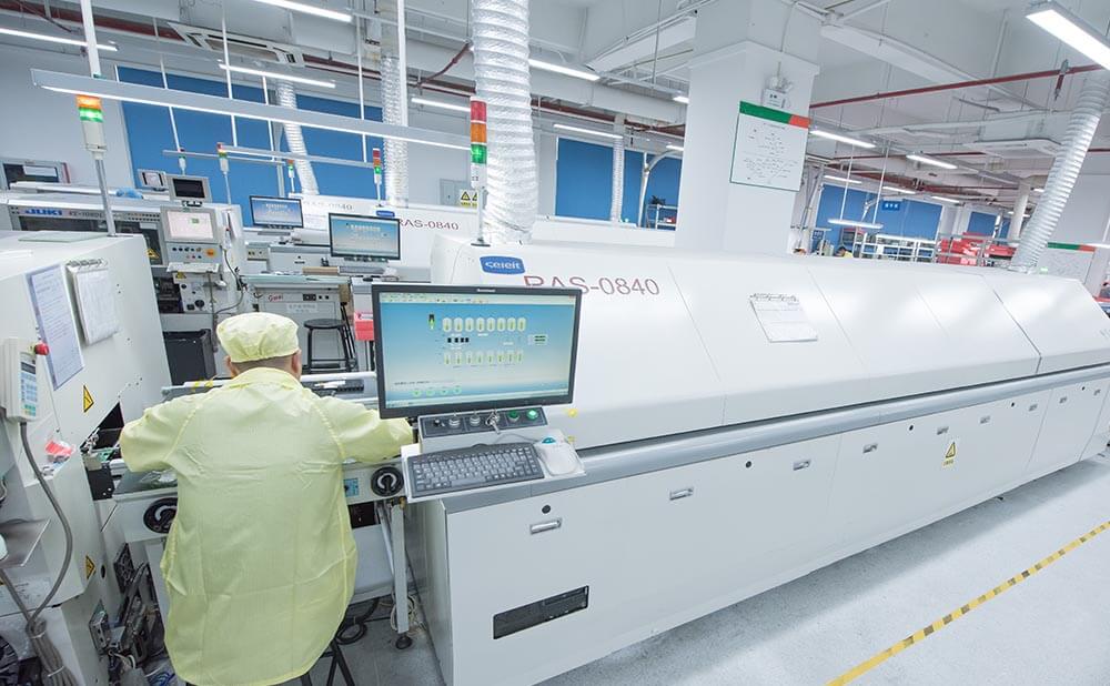
8 Temperature zone reflow oven
Once the components are all in place, they need firmly attaching to the board. This occurs during the soldering process, where a material called ‘solder’ is melted to form conductive connections between the parts and their pads.
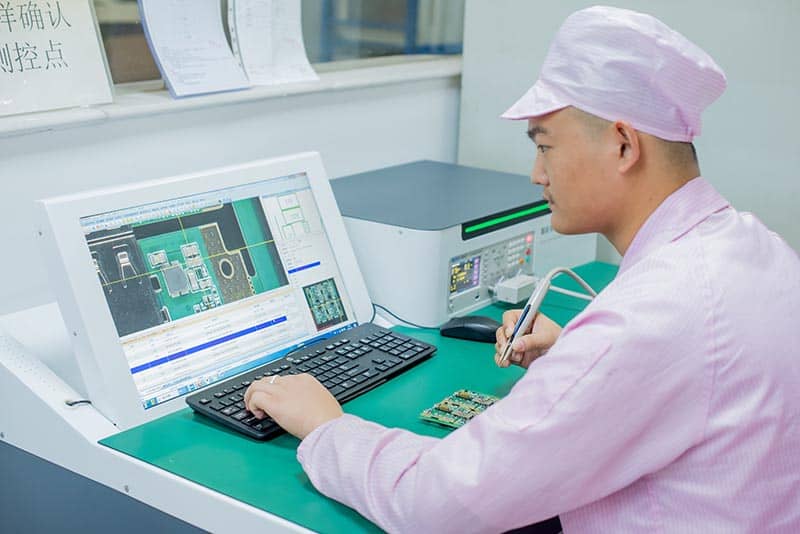
PCBA inspection equipment
Once the board is completed, manufacturers need to ensure that no parts are faulty and that the board works as intended. This means checking for performance as well as interrupted electrical connections.
First article inspection (FAI)
FAI can be understood as the first piece quality inspection before the start of mass pcb assembly.
Is to avoid the large quantities defective that because of the process,operation or other reasons.
Each resistor,capacitance and inductance will be inspected by LCR meter.
The chips verified by QC with BOM and Assembly drawing.
Automatic optic inspection(AOI)
AOI device is for inspection the compoents placement and solder joint quality after SMT(Surface Mounted Technology).
To achieve better quality control,find and remove the errors early in the assembly process.
It is avoid the defective product to assembly,will avoid scrapping the repairable circuit board.

X-Ray inspection
X-ray is a very short wavelength of electromagnetic waves, the wavelength range of 0.0006 a 80nm,
with a strong penetration,X-ray could penetrate a variety of different density of the material.
When the design have BGA or QFN,for checking the solder quality that could not be visible by eyes.
We will use X-ray machine to inspect the BGA or QFN package in finished PCB assembly.

Final quality assuerance (FQA)
After all the above quality control processes, quality Engineer will make final quality visual inspection for the all product.

Functional test
Functional Test are based on automated test tools to simulate a variety of normal, peak and abnormal load
conditions to test the performance of the final PCB assembly products.
Functional Test is a complex process,which include Tool made,Programming and testing,
need technicality support from customer.
