
Skip to content
Andwin Circuits
  • Home
  • ProductsExpand
    • HDI multilayer PCB
    • Rigid Flex PCB
    • Flex pcb
    • Special PCBExpand
      • High Frequency PCBExpand
        • Rogers RO4350B PCB
        • Rogers RO4003 pcb
        • Rogers RO3003 PCB
        • Rogers 5880 PCB
        • DICLAD 527 PCB
        • Taconic TLX series
        • Taconic TLX-8 RF PCB
        • Taconic TLX-9 RF PCB
      • High speed pcbExpand
        • Megtron 6 High Speed PCB
        • TU-872 SLK Sp High Speed
      • High TG PCBExpand
        • SHENGYI SH260 PCB
        • ISOLA 370HR PCB
        • ISOLA IS410 PCB
        • ISOLA IS420 PCB
      • Heavy copper PCB
      • Copper coin pcb
      • Copper inlay PCB
    • Metal Core PCBExpand
      • Copper core pcb
      • Aluminum PCB
      • 2 Layers Aluminum PCB
      • Direct thermal MCPCB
      • 2 Layers Direct Thermal
    • Ceramic PCBExpand
      • DPC ceramic PCB
      • DBC ceramic PCB
      • Thick film Ceramic PCB
      • Al2O3 Alumina PCB
      • AIN ALN ceramic PCB
      • IGBT Ceramic PCB
  • ServiceExpand
    • PCB Assembly
    • Quick turn PCB assembly
    • PCBA conformal coating
  • IndustryExpand
    • Telecommunication
    • IoT and Wireless
    • Industrial Control
    • Thermal management
    • Power and Energy
    • IC test board
    • Automative
    • Medical
  • CapabilityExpand
    • Rigid PCB
    • Rigid flex PCB
    • Metal core PCB
    • PCB Assembly
  • TechnologyExpand
    • Blogs
    • Via in pad
    • PCB E-test
    • PCB stack up
    • MCPCB panelization
    • Controlled impedance PCB
  • AboutExpand
    • About us
    • Certification
    • Factory Tour
  • Contact
Andwin Circuits
Home / PCB Assembly: Essential Circuit Board Design Tips for Optimal Performance

PCB Assembly: Essential Circuit Board Design Tips for Optimal Performance

ByGrace July 25, 2025July 24, 2025

Printed Circuit Board (PCB) assembly is a critical process in electronics manufacturing, where design decisions significantly impact functionality, reliability, and cost. Whether you’re designing a simple single-layer board or a complex multi-layer PCB, following best practices ensures smooth assembly and high performance. This article explores key PCB design techniques to optimize manufacturability, signal integrity, and assembly efficiency.
Contact us for PCB quote now |

1. Component Placement Strategies

1.1 Group Related Components Together

  • Place components logically based on their function (e.g., power supply section, analog circuits, digital circuits).
  • Minimize trace lengths between connected components to reduce signal interference and parasitic effects.

1.2 Consider Thermal Management

  • Position heat-generating components (e.g., voltage regulators, power transistors) away from sensitive ICs.
  • Use thermal vias and copper pours to dissipate heat efficiently.

1.3 Optimize for Automated Assembly

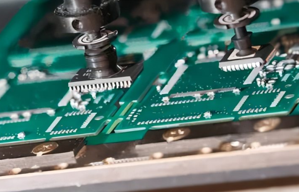
  • Ensure components are aligned in the same orientation for pick-and-place machines.
  • Avoid placing tall components near small ones to prevent assembly interference.

2. Routing and Signal Integrity

2.1 Follow Proper Trace Width and Spacing Rules

  • Use appropriate trace widths based on current requirements (e.g., wider traces for high-power paths).
  • Maintain sufficient clearance between traces to prevent crosstalk and short circuits.

2.2 Minimize Signal Path Lengths

  • Keep high-speed signal traces (e.g., clock lines, differential pairs) as short as possible.
  • Use impedance-controlled routing for RF and high-frequency signals.

2.3 Avoid Sharp Angles in Traces

  • Use 45° angles or curved traces instead of 90° turns to reduce electromagnetic interference (EMI).

2.4 Proper Grounding Techniques

  • Implement a solid ground plane to minimize noise and improve signal integrity.
  • Avoid ground loops by ensuring a low-impedance return path.

3. Design for Manufacturability (DFM)

3.1 Adhere to Manufacturer’s Design Rules

  • Follow the PCB fabricator’s guidelines for minimum trace width, hole size, and spacing.
  • Ensure proper annular ring sizes for vias and plated through-holes.

3.2 Panelization for Efficient Assembly

  • Include fiducial markers and tooling holes for accurate PCB alignment during assembly.
  • Use breakaway tabs or V-grooves for easy depanelization after assembly.

3.3 Silkscreen and Assembly Markings

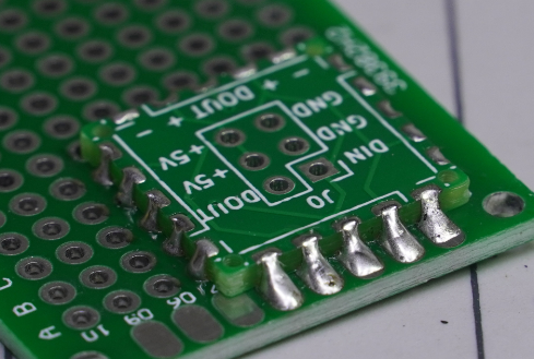
  • Clearly label component designators, polarity indicators, and pin-1 markers.
  • Avoid placing silkscreen over pads or vias to prevent assembly errors.
4. Power Distribution and Decoupling

4.1 Use Proper Power Plane Design

  • Implement dedicated power planes for stable voltage distribution.
  • Avoid splitting power planes unless necessary, as it can increase impedance.

4.2 Place Decoupling Capacitors Close to ICs

  • Use 0.1 µF capacitors near power pins to filter high-frequency noise.
  • Add bulk capacitors (10 µF or higher) near voltage regulators for stable supply.

5. Testability and Debugging Considerations

5.1 Include Test Points

  • Add accessible test points for critical signals to facilitate debugging.
  • Use through-hole test points for reliable probe contact.

5.2 Design for In-Circuit Testing (ICT)

  • Ensure test pads are large enough for bed-of-nails fixtures.
  • Avoid placing components too close to test points.

6. Avoiding Common PCB Assembly Pitfalls

6.1 Incorrect Footprint Selection

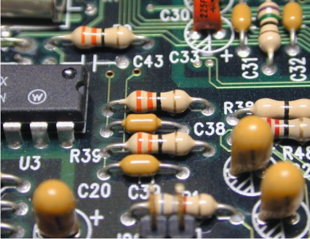
  • Double-check component footprints against datasheets to prevent soldering issues.
  • Verify pad sizes for surface-mount devices (SMDs).

6.2 Insufficient Solder Mask Clearance

  • Ensure solder mask openings are slightly larger than pads to prevent solder bridging.

6.3 Poor Via Placement

  • Avoid placing vias in pad centers, as they can cause solder wicking issues.
  • Use tented vias to prevent solder migration.
Contact us for PCB quote now |

Conclusion

Designing a PCB for efficient assembly requires careful planning, adherence to DFM guidelines, and attention to signal integrity. By optimizing component placement, routing, power distribution, and testability, engineers can ensure reliable, high-performance PCB assemblies. Following these best practices minimizes manufacturing defects, reduces costs, and accelerates time-to-market for electronic products.

Would you like additional details on any specific aspect of PCB assembly design?

Contact us for PCB quote now |
Post Tags: #aluminum clad pcb#aluminum core pcb#aluminum core pcb led#aluminum pcb#assemble pcb#pcb assembly#pcb design#PCB layout

Post navigation

Previous Previous
Impact of Different pcb and component deploy for thermal behavior
NextContinue
Case Study on Methods to Prevent Defects in PCB Manufacturing

Search

Search

Products

  • HDI Multilayer PCB
  • Rigid Flex PCB
  • Flex pcb
  • High Frequency PCB
  • High speed pcb
  • Heavy copper PCB
  • Metal Core PCB
  • Ceramic PCB

Address

Andwin Circuits Co.,Limited
Email: sales@andwinpcb.com
Tel: +86 755 2832 9394
Fax:+86 755 2992  6717
ADD:1-2F-1217,HouDeQun Industrial park,
NanTing RD NO.56,ShaJing,BaoAn,Shenzhen 518104,GuangDong,China

Products

  • HDI Multilayer PCB
  • Rigid Flex PCB
  • Flex pcb
  • High Frequency PCB
  • High speed pcb
  • Heavy copper PCB
  • Metal Core PCB
  • Ceramic PCB

Technology

  • Blogs
  • Via in pad
  • PCB E-test
  • PCB stack up
  • Metal core PCB panelization
  • Controlled impedance PCB

CERTIFICATION

Certification >>


Copyright© 2003 - 2026 Andwin | All Rights Reserved | Powered by Andwin

Scroll to top
  • Home
  • Products
    • HDI multilayer PCB
    • Rigid Flex PCB
    • Flex pcb
    • Special PCB
      • High Frequency PCB
        • Rogers RO4350B PCB
        • Rogers RO4003 pcb
        • Rogers RO3003 PCB
        • Rogers 5880 PCB
        • DICLAD 527 PCB
        • Taconic TLX series
        • Taconic TLX-8 RF PCB
        • Taconic TLX-9 RF PCB
      • High speed pcb
        • Megtron 6 High Speed PCB
        • TU-872 SLK Sp High Speed
      • High TG PCB
        • SHENGYI SH260 PCB
        • ISOLA 370HR PCB
        • ISOLA IS410 PCB
        • ISOLA IS420 PCB
      • Heavy copper PCB
      • Copper coin pcb
      • Copper inlay PCB
    • Metal Core PCB
      • Copper core pcb
      • Aluminum PCB
      • 2 Layers Aluminum PCB
      • Direct thermal MCPCB
      • 2 Layers Direct Thermal
    • Ceramic PCB
      • DPC ceramic PCB
      • DBC ceramic PCB
      • Thick film Ceramic PCB
      • Al2O3 Alumina PCB
      • AIN ALN ceramic PCB
      • IGBT Ceramic PCB
  • Service
    • PCB Assembly
    • Quick turn PCB assembly
    • PCBA conformal coating
  • Industry
    • Telecommunication
    • IoT and Wireless
    • Industrial Control
    • Thermal management
    • Power and Energy
    • IC test board
    • Automative
    • Medical
  • Capability
    • Rigid PCB
    • Rigid flex PCB
    • Metal core PCB
    • PCB Assembly
  • Technology
    • Blogs
    • Via in pad
    • PCB E-test
    • PCB stack up
    • MCPCB panelization
    • Controlled impedance PCB
  • About
    • About us
    • Certification
    • Factory Tour
  • Contact
Search