
PCB Board Ground Return Path Handling: Best Practices and Design Considerations
Introduction
Printed Circuit Board (PCB) design is a critical aspect of modern electronics, influencing signal integrity, electromagnetic compatibility (EMC), and overall system performance. One of the most crucial yet often overlooked aspects of PCB design is the proper handling of ground return paths. A poorly designed return path can lead to signal degradation, increased electromagnetic interference (EMI), and even circuit malfunction.
This article explores the fundamentals of ground return paths in PCBs, discusses common challenges, and provides best practices to optimize return path design for improved signal integrity and reduced noise.
1. Understanding Ground Return Paths in PCBs
1.1 What is a Return Path?
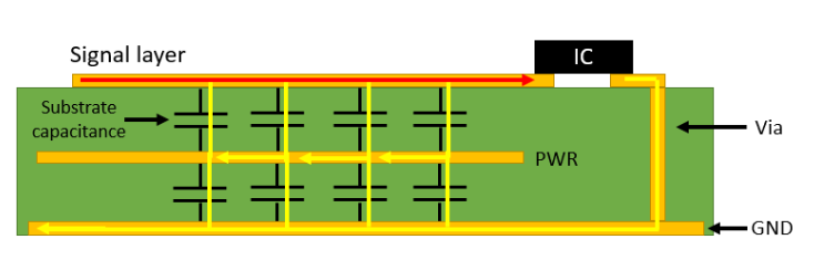
In a PCB, current flows from a source to a load and must return to its origin through a closed loop. The path taken by the returning current is called the return path. For DC and low-frequency signals, the return path is typically the ground plane. However, at high frequencies, return currents follow the path of least impedance, which often means staying directly beneath the signal trace.
1.2 Why is the Return Path Important?
A well-designed return path ensures:
- Signal Integrity (SI): Minimizes signal distortion and reflections.
- Electromagnetic Compatibility (EMC): Reduces radiated emissions and susceptibility to interference.
- Power Integrity (PI): Ensures stable power delivery with minimal noise.
If the return path is disrupted (e.g., due to splits in the ground plane), the current is forced to take a longer route, increasing loop inductance and EMI.
2. Key Challenges in Ground Return Path Design
2.1 Split Ground Planes
Many PCBs use multiple ground planes (e.g., analog and digital grounds). If not properly connected, return currents may take detours, leading to:
- Increased loop area → Higher EMI.
- Ground bounce → Noise coupling between circuits.
Solution: Use a single solid ground plane where possible. If splits are necessary, ensure proper stitching (e.g., with capacitors or ferrite beads) to provide a low-impedance return path.
2.2 High-Speed Signals and Return Current Proximity
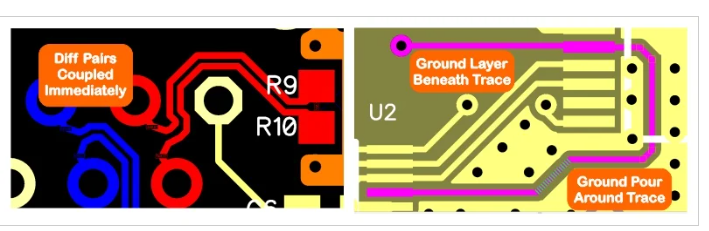
At high frequencies (>1 MHz), return currents flow directly beneath the signal trace due to mutual inductance. If the ground plane is interrupted (e.g., by a slot or gap), the return current is forced to take a longer path, increasing inductance and crosstalk.
Solution:
- Avoid routing high-speed signals over gaps in the ground plane.
- Use continuous ground planes beneath critical traces.
- Implement via stitching to ensure a low-impedance return path across layers.
2.3 Mixed-Signal PCB Design
Mixed-signal PCBs (combining analog and digital circuits) require careful ground separation to prevent noise coupling. However, improper partitioning can worsen return path issues.
Solution:
- Use a single ground plane with careful component placement to minimize interference.
- If separate grounds are needed, connect them at a single point (star grounding).
3. Best Practices for Optimizing Ground Return Paths
3.1 Use a Solid Ground Plane
A continuous ground plane provides the lowest impedance return path.
- Multilayer PCBs: Dedicate one or more layers to ground.
- 2-Layer PCBs: Maximize ground copper pour and minimize splits.
3.2 Minimize Return Path Loops
- Route high-speed signals adjacent to their return paths.
- Avoid unnecessary vias that force return currents to change layers.
3.3 Proper Via Placement for Multi-Layer PCBs
When a signal transitions between layers, its return current must follow. Poor via placement can disrupt the return path.
Solution:
- Place ground vias near signal vias to provide a continuous return path.
- Use return path stitching for high-speed signals.
3.4 Avoid Ground Loops
Ground loops occur when multiple return paths create circulating currents, leading to noise.
Solution:
- Use a star grounding topology for sensitive circuits.
- Ensure proper grounding in power supply layouts.
3.5 Controlled Impedance Routing
For high-speed signals (e.g., DDR, USB, PCIe), controlled impedance traces must have a well-defined return path.
Solution:
- Use microstrip or stripline configurations with reference planes.
- Maintain consistent dielectric spacing for impedance control.
4. Advanced Techniques for Return Path Optimization
4.1 Embedded Capacitance for High-Speed Designs
Embedded capacitance (e.g., power-ground plane coupling) reduces high-frequency return path impedance.
4.2 Differential Pair Routing
Differential signals (e.g., USB, HDMI) cancel out common-mode noise, but return path consistency is still critical.
Solution:
- Ensure both traces in a pair have symmetric return paths.
- Avoid referencing different ground planes for each trace.
4.3 Simulation and Analysis
Use EM simulation tools (e.g., Ansys HFSS, Cadence Sigrity) to analyze return current distribution and identify discontinuities.
5. Common Mistakes and How to Avoid Them
| Mistake | Impact | Solution |
|---|---|---|
| Splitting ground planes without stitching | Increased EMI, signal integrity issues | Use ground vias or capacitors for stitching |
| Routing high-speed signals over gaps | Increased loop inductance | Keep signals over continuous ground |
| Poor via placement for layer transitions | Disrupted return current | Place ground vias near signal transitions |
| Ignoring mixed-signal grounding | Noise coupling between analog and digital circuits | Use a single ground plane or proper partitioning |
6. Conclusion
Proper handling of PCB ground return paths is essential for signal integrity, EMC, and overall circuit reliability. By following best practices—such as using solid ground planes, minimizing return path loops, and optimizing via placement—designers can significantly reduce noise and improve performance.
For high-speed and mixed-signal designs, advanced techniques like embedded capacitance and simulation-based analysis further enhance return path efficiency. By understanding and implementing these principles, engineers can ensure robust and reliable PCB designs.