
PCB Digital Circuit Anti-Interference Techniques
Abstract
With the increasing complexity and speed of digital circuits, electromagnetic interference (EMI) and noise have become critical challenges in printed circuit board (PCB) design. Effective anti-interference techniques are essential to ensure signal integrity, reduce crosstalk, and improve system reliability. This paper discusses the sources of interference in digital circuits, analyzes key anti-interference design strategies, and provides practical PCB layout and routing techniques to minimize noise and enhance performance.
1. Introduction
Digital circuits are widely used in modern electronics, from consumer devices to industrial control systems. However, high-speed signal transmission, switching noise, and electromagnetic coupling can introduce interference, leading to signal distortion, timing errors, and even system failures. To mitigate these issues, PCB designers must implement robust anti-interference measures.
This paper explores the primary sources of interference in digital circuits, examines key design principles for noise reduction, and presents best practices for PCB layout, grounding, shielding, and filtering.
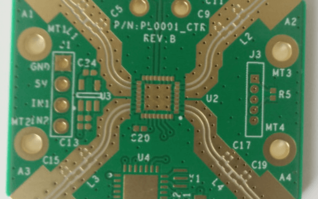
2. Sources of Interference in Digital Circuits
Interference in digital circuits arises from multiple sources, including:
2.1 Conducted Noise
- Power Supply Noise: Voltage fluctuations due to switching currents in power lines.
- Ground Bounce: Voltage spikes caused by high-speed switching in ground planes.
- Signal Crosstalk: Unwanted coupling between adjacent traces due to mutual inductance and capacitance.
2.2 Radiated Noise
- Electromagnetic Interference (EMI): High-frequency signals radiating from traces, connectors, or components.
- Electrostatic Discharge (ESD): Sudden voltage spikes from static electricity.
2.3 Internal Circuit Noise
- Switching Noise: Transient currents from logic gate transitions.
- Clock Jitter: Timing variations due to noise in clock distribution networks.
3. Key Anti-Interference Design Strategies
3.1 Proper Grounding Techniques
- Single-Point vs. Multi-Point Grounding:
- Single-point grounding is suitable for low-frequency circuits to avoid ground loops.
- Multi-point grounding is preferred for high-frequency circuits to reduce impedance.
- Ground Plane Design:
- Use a solid ground plane to minimize ground impedance and noise.
- Separate analog and digital ground planes, connecting them at a single point.
3.2 Power Supply Decoupling
- Bypass Capacitors: Place decoupling capacitors (0.1µF – 10µF) near IC power pins to filter high-frequency noise.
- Ferrite Beads: Use ferrite beads in power lines to suppress high-frequency EMI.
- Voltage Regulators: Implement low-noise regulators for sensitive analog circuits.
3.3 Signal Integrity and Impedance Control
- Controlled Impedance Routing: Match trace impedance to prevent reflections (e.g., 50Ω for single-ended, 100Ω for differential pairs).
- Termination Techniques: Use series or parallel termination to reduce signal reflections in high-speed lines.
3.4 Shielding and EMI Reduction
- Faraday Cages: Enclose sensitive circuits in conductive shielding to block external EMI.
- Guard Traces: Place grounded guard traces between high-speed signals to reduce crosstalk.
- EMI Filters: Install filters on I/O lines to suppress conducted noise.
3.5 PCB Layout Best Practices
- Component Placement:
- Group related components (e.g., analog, digital, RF) to minimize interference.
- Keep high-speed traces short and away from noise sources.
- Trace Routing:
- Avoid right-angle bends (use 45° or curved traces).
- Maintain sufficient spacing between traces to reduce crosstalk.
- Route critical signals (clocks, differential pairs) first.
- Layer Stackup:
- Use multilayer PCBs with dedicated power and ground planes.
- Route high-speed signals on inner layers between ground planes for shielding.
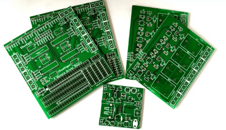
4. Advanced Anti-Interference Techniques
4.1 Differential Signaling
- Reduces common-mode noise by transmitting complementary signals (e.g., USB, Ethernet).
4.2 Spread Spectrum Clocking (SSC)
- Reduces EMI by modulating the clock frequency.
4.3 Optical Isolation
- Uses optocouplers to isolate noisy digital circuits from sensitive analog sections.
4.4 Simulation and Testing
- Perform signal integrity (SI) and power integrity (PI) simulations before fabrication.
- Use spectrum analyzers and oscilloscopes to measure noise and EMI.
5. Conclusion
Designing PCB digital circuits with strong anti-interference capabilities is crucial for reliable operation. By implementing proper grounding, power decoupling, shielding, and careful routing, engineers can significantly reduce noise and EMI. Advanced techniques such as differential signaling, optical isolation, and simulation further enhance circuit robustness.
Future trends in PCB design will focus on higher-speed interfaces (e.g., PCIe 5.0, DDR5) and advanced materials to further mitigate interference challenges.