
PCB Optimization Based on DFM and DFT Guidelines
Optimizing any PCB design requires a great deal of effort. Proper PCB inspection is essential when preparing for the production phase. Therefore, all designers’ goals ultimately revolve around the goals of enhanced functionality, ease of manufacturing, and ease of testing. Optimizing a PCB for manufacturing involves thoroughly analyzing potential improvements to the PCB and testing issues that could affect manufacturing.
Contract Manufacturer (CM) Design for Manufacturing (DFM) is the principle of evaluating the likelihood of potential problems that may arise during the manufacturing process. Evaluating the feasibility of a PCB based on DFM involves the following preliminary steps.
Design for Manufacturing (DFM) Evaluation
l Design Review: After your CM initially receives your design data, your design will receive an evaluation or design review. The format you use for data transfer determines how your CM will proceed.
l Format Evaluation: If your design uses a CAD database format, it will go directly to an engineering technical evaluation. However, if it uses another format, it will usually require importing, which will increase processing time. It is important to know in advance which formats your CM considers reliable or acceptable.
l Component Evaluation: Your CM will evaluate your bill of materials (BOM) to determine which components are about to reach the end of their life (EOL) or require a longer lead time. The purpose of component evaluation is to eliminate components that do not meet the recommended manufacturing standards.
l Component Availability Evaluation: Your CM will match the listed components to a master component database that will provide information on real-time component availability. This information is continuously updated and enables the CM to make accurate recommendations for any necessary component replacements. If an exact match does not exist for your component due to end-of-life (EOL), the CM will use this database to suggest an appropriate functional replacement.
In addition to these initial checks, your CM will evaluate the following factors to assess the overall manufacturability of the design.
Factors Evaluating PCB Manufacturability
Component Spacing: When components are placed too close together, it creates issues with automated pick and place and adversely affects testing (fixtures).
Component Placement (Position and Rotation): Component placement affects every aspect of PCB design. Therefore, where and how you place components also affects the solderability of the board. If a larger component is positioned in front of a smaller component before it fluctuates, it will shadow that component and can cause solder joint issues.
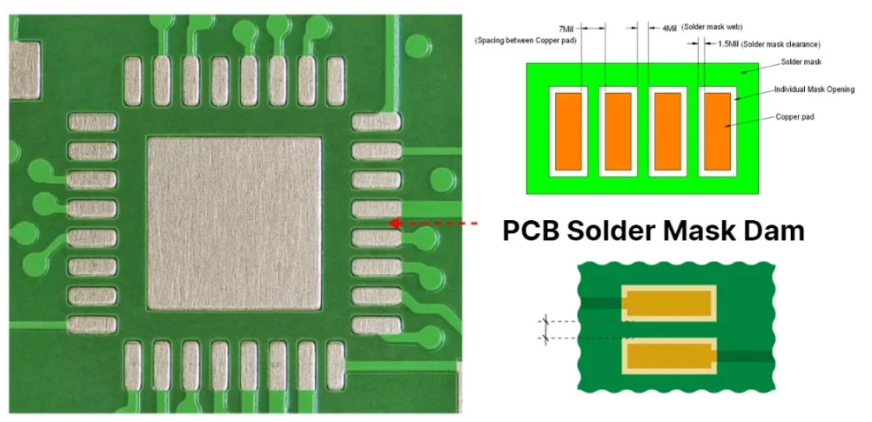
Missing Solder Mask Between Pads: Shorts (electrical) between pins occur due to bridging during assembly.
Improper surface mount pad size: This will result in tombstoning. This is when a component such as a capacitor or resistor partially lifts off the pad at one end.
Acid trapping: Routing traces at sharp angles can cause problems in removing etching chemicals from the PCB, which can contribute to PCB manufacturing issues.
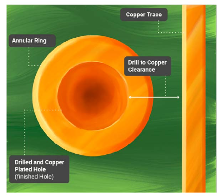
Drill optimization: Uniform drill sizes are incorporated, which reduces the number of drill sizes in use. Optimizing drills can reduce manufacturing costs.
In addition to checking for manufacturability and functionality, your CM will evaluate the data provided for testability according to the principles of Design for Testability (DFT). This involves evaluating the design against DFT guidelines.
Design for Testability (DFT) Guidelines for PCBs
Testability affects many areas of PCB design. Overall, this includes building or modifying test fixtures (if needed), test point pads (in-circuit testing), and component spacing relative to the edge of the board (pitch). During the process of evaluating the design for testability, your CM will reference the test specifications you provide. The information gleaned from this data enables the CM to develop a workaround to address the board specifications. You can optimize the DFT process and help your CM by completing the following actions:
Provide markups on the schematic to include connection points and test points in each test review in addition to evaluating the layout.
Include specific test points in the scheme to help the CM with this preparation. Overall, the design evaluation and test approach will help determine the type of fixture required. This helps determine if the design needs to be modified to increase successful fault coverage of the test process.
Work with your CM to incorporate all relevant test information into a test description (TI) document, which should include illustrations and instructions used during the test process.
Understand and evaluate the types of tests available to make informed design decisions and optimize the test process. Tests have specific advantages and disadvantages, so it is important to be familiar with the test specifications.
For example, Flying Probe Testing is best suited for prototyping or low-volume production because it is easy to set up for testing. However, Flying Probe Testing is slower than ICT. In addition, In-Circuit Test (ICT) fixtures and fixed programming are also best suited for high-volume production of proven PCB designs. Choosing the right test type can have a significant impact on overall results.
Testability: Testability affects many areas of a PCB design. In general, this includes building or modifying test fixtures (if needed), test point pads (in-circuit testing), and component spacing relative to the edge of the board (spacing).
Your CM can technically develop test specifications; however, doing so for your design requires you to work closely with them and provide as much information as necessary about the circuit’s operation and functionality. Due diligence at this stage is critical to ensure that the PCB is fully tested and meets your expectations. It is also important to follow PCB layout guidelines to enhance testability.
PCB Layout Guidelines to Optimize Testability
Here are key considerations regarding PCB layout to ensure testability of your design:
In-circuit test points should be located on every net of your design to ensure full test coverage.
All test points should have 50 mil clearance from pads and components.
All test points should have 100 mil clearance from the edge of the board.
It should be possible to perform in-circuit testing on both sides of the board at once, and I recommend setting this up with your CM up front.
Optimizing PCBs for Cost-Effectiveness
Optimizing your design for testability can reduce overall costs. Expenses incurred during PCB production can be broadly divided into the following four categories:
- Parts costs
- Blank PCB manufacturing costs
- Testing costs
- Assembly costs
While the four major categories of expenses can vary greatly depending on the exact design specifications, testing costs can amount to 25% or even up to 30% of the total cost of a completed PCB. Therefore, your design must fully incorporate DFT and DFM. The overall goal is to design a highly testable PCB while providing the ability to quickly isolate issues related to component failures and manufacturing errors. Optimization of DFM and DFT can only be truly achieved when you work with a CM.