PCB Pad Design Standards: A Comprehensive Guide
Introduction to PCB Pad Design
Printed Circuit Board (PCB) pad design is one of the most critical aspects of PCB layout that directly affects the manufacturability, reliability, and performance of electronic assemblies. Pads serve as the connection points between component leads and the conductive traces on the PCB. Proper pad design ensures strong mechanical bonds, reliable electrical connections, and facilitates efficient manufacturing processes.
This article explores the essential standards, guidelines, and best practices for PCB pad design, covering various component types, manufacturing considerations, and industry standards that govern pad geometry and layout.
Importance of Proper Pad Design
Well-designed pads are fundamental to PCB quality for several reasons:
- Soldering Quality: Proper pad dimensions ensure adequate solder fillet formation
- Mechanical Strength: Correct pad sizes provide sufficient bonding area
- Thermal Management: Pads help dissipate heat from components
- Manufacturing Yield: Properly designed pads reduce assembly defects
- Reliability: Good pad design prevents tombstoning, bridging, and other soldering defects
Industry Standards for PCB Pad Design
Several industry standards provide guidelines for PCB pad design:
- IPC-7351: Generic Requirements for Surface Mount Design and Land Pattern Standards
- IPC-SM-782: Surface Mount Design and Land Pattern Standard (superseded by IPC-7351)
- IPC-2221/2222: Generic/rigid PCB design standards with pad requirements
- IEC 61188-7: International standard for electronic assembly technology
- J-STD-001: Requirements for Soldered Electrical and Electronic Assemblies
These standards provide formulas and tables for calculating appropriate pad dimensions based on component sizes and manufacturing processes.
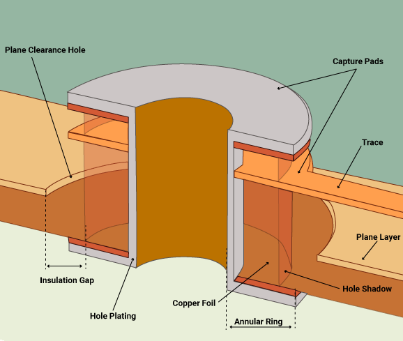
Through-Hole Pad Design Standards
Basic Through-Hole Pad Parameters
- Hole Size: Typically 0.25-0.5mm larger than lead diameter
- For wave soldering: +0.2-0.4mm
- For hand soldering: +0.4-0.6mm
- Pad Diameter: Minimum annular ring of 0.15mm (preferably 0.25mm)
- Standard pad diameter = hole diameter + (2 × annular ring requirement)
- Thermal Relief: For ground/power planes, use spoke connections (typically 4, 0.2-0.3mm wide)
Common Through-Hole Components
- Axial Lead Components:
- Pad diameter: lead diameter + 0.8mm minimum
- Hole size: lead diameter + 0.4mm
- Radial Lead Components:
- Similar to axial but with closer spacing
- DIP Components:
- Pad diameter: 1.8-2.0mm for standard DIPs
- Hole size: 0.8-1.0mm for standard leads
Surface Mount Pad Design Standards
SMD Pad Design Considerations
- Component Termination Type:
- Gull wing (SOIC, QFP)
- J-lead (PLCC, SOJ)
- Ball grid array (BGA)
- Chip components (resistors, capacitors)
- Solder Joint Requirements:
- Minimum and maximum solder fillet requirements
- Solder volume considerations
- Thermal Balance:
- Equal heat dissipation on both ends to prevent tombstoning
Common SMD Pad Types
- Rectangular Pads (Chip Components):
- Length: component length + 0.2-0.5mm
- Width: component width ±0.1mm
- Spacing: component dimension minus tolerance
- Gull Wing Pads (SOIC, QFP):
- Pad extends 0.3-0.5mm beyond lead
- Width matches lead width or slightly wider
- J-Lead Pads (PLCC):
- Pad extends under component body
- Curved pad shape to match lead
- BGA Pads:
- Typically same size as ball diameter (or 80-90% of ball size)
- Solder mask defined or non-solder mask defined designs
IPC-7351 Land Pattern Naming Convention
The IPC-7351 standard defines three density levels for land patterns:
- Density Level A (Maximum):
- Largest pad sizes
- For low-density designs or hand assembly
- Density Level B (Median):
- Balanced between size and spacing
- For most commercial applications
- Density Level C (Minimum):
- Smallest pad sizes
- For high-density designs with automated assembly
The naming convention includes:
- Component type
- Lead/pitch dimensions
- Density level
- Example: “RESC1608L” (Chip resistor, 1608 metric, Level L – Least)
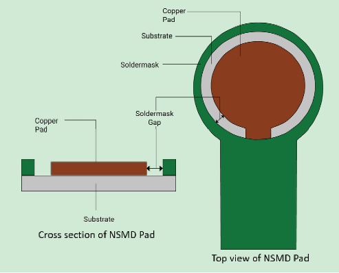
Solder Mask and Paste Mask Design
Solder Mask Design
- Solder Mask Clearance:
- Typically 0.05-0.1mm beyond pad
- For BGAs: may be same size as pad (solder mask defined)
- Solder Mask Bridges:
- Minimum 0.1mm between pads
- Solder Mask Material:
- Liquid Photoimageable (LPI) most common
- Dry film for some applications
Solder Paste Design
- Stencil Aperture Design:
- Typically 80-100% of pad area
- May be reduced for fine-pitch components
- Aperture Shape:
- Rectangular for most components
- Home-plate for fine-pitch QFPs
- Area Ratio:
- Should be >0.66 for good paste release
- (Aperture area)/(aperture wall area)
Special Pad Designs
Thermal Pads
- Purpose: Heat dissipation for high-power components
- Design Features:
- Large copper area
- Multiple vias to inner/opposite layers
- May connect to heat sinks
- Thermal Relief Connections:
- Spoke connections to prevent heat sinking during soldering
Castellated Pads
- Purpose: For module-to-board connections
- Design Features:
- Half holes at board edges
- Plated with solderable finish
- Typically 0.5-1.0mm pitch
Test Pads
- Purpose: For manufacturing test probes
- Design Requirements:
- Minimum 0.8mm diameter
- Clear of obstructions
- Preferably on bottom side
Design for Manufacturing (DFM) Considerations
- Pad-to-Pad Spacing:
- Minimum 0.2mm for wave soldering
- May be less for reflow-only assemblies
- Pad-to-Trace Clearance:
- Minimum 0.15mm for standard designs
- Copper Balance:
- Similar copper area on both sides to prevent warpage
- Fiducial Marks:
- Global fiducials: 1-3mm diameter
- Local fiducials: 1mm diameter
- Clearance: 2x diameter
High-Density Interconnect (HDI) Pad Design
- Microvia Pads:
- Typically 0.1-0.2mm diameter
- Capture pads 0.25-0.3mm
- Fine-Pitch Components:
- 0.4mm pitch and below
- May use dog-bone or via-in-pad designs
- Via-in-Pad:
- Filled and planarized vias
- Copper cap for surface finish
Surface Finishes and Pad Design
Different surface finishes affect pad design:
- HASL (Hot Air Solder Leveling):
- Adds 0.02-0.05mm to pad height
- May require larger pads for fine-pitch
- ENIG (Electroless Nickel Immersion Gold):
- Flat surface, good for fine-pitch
- Nickel thickness 3-6μm, gold 0.05-0.1μm
- OSP (Organic Solderability Preservative):
- Flat surface, temporary protection
- Immersion Silver/Tin:
- Flat surface, good solderability
Design Verification and Validation
- DFM Checks:
- Automated design rule checks (DRC)
- Annular ring verification
- Solder mask clearance checks
- Prototype Testing:
- Solderability tests
- Thermal cycling
- Mechanical stress tests
- Process Validation:
- Solder paste inspection (SPI)
- Automated optical inspection (AOI)
- X-ray inspection for BGAs
Emerging Trends in Pad Design
- Smaller Components:
- 01005 (0.4mm × 0.2mm) and smaller chip components
- Advanced Packages:
- Wafer-level chip-scale packages (WLCSP)
- 3D packaging with micro-bumps
- Embedded Components:
- Components within PCB layers
- Special pad designs for buried components
- Additive Manufacturing:
- Printed electronics with unique pad geometries
Conclusion
Proper PCB pad design is essential for creating reliable, manufacturable electronic assemblies. By following industry standards like IPC-7351 and considering manufacturing requirements, designers can optimize pad geometries for their specific applications. As components continue to shrink and packaging technologies evolve, pad design remains a critical factor in PCB layout that requires careful attention to detail and ongoing adaptation to new technologies.
The key to successful pad design lies in balancing the competing demands of electrical performance, mechanical reliability, and manufacturing feasibility while staying current with evolving industry standards and technological advancements.