
PCB Panelization: Methods and Design Rules
Introduction
Printed Circuit Board (PCB) panelization is a crucial step in PCB manufacturing that involves arranging multiple PCBs on a single panel to optimize production efficiency, reduce costs, and improve handling during assembly. Panelization ensures that smaller or irregularly shaped PCBs can be processed efficiently in automated assembly lines. This article explores different PCB panelization methods, key design rules, and best practices for successful panelization.
Why Panelization is Necessary
- Manufacturing Efficiency – Fabricating multiple PCBs on a single panel reduces material waste and speeds up production.
- Assembly Handling – Small or flexible PCBs are difficult to handle individually; panelization allows automated pick-and-place machines to process them efficiently.
- Cost Reduction – Fewer panels mean lower setup costs and reduced labor expenses.
- Improved Yield – Proper panelization minimizes breakage and defects during fabrication and assembly.
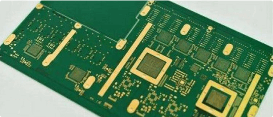
Common PCB Panelization Methods
1. Tab Routing (V-Scoring + Breakaway Tabs)
Tab routing is the most widely used panelization method. It involves connecting PCBs using small tabs (also called “mouse bites”) and scoring lines (V-grooves) for easy separation after assembly.
- V-Scoring (V-Grooves): A V-shaped groove is cut between PCBs, leaving a thin layer of material (typically 1/3 of the board thickness) to hold the panels together. After assembly, the boards can be easily snapped apart.
- Breakaway Tabs: Small perforated tabs (with drilled holes) connect PCBs, allowing easy depanelization by breaking or cutting.
Advantages:
✔ Cost-effective
✔ Suitable for rectangular PCBs
✔ Minimal material waste
Disadvantages:
✖ Not ideal for irregular shapes
✖ May require manual breaking, risking damage
2. Solid Tab Panelization
Instead of perforated tabs, solid tabs (without mouse bites) are used to hold PCBs together. This method is used when extra strength is needed during assembly.
Advantages:
✔ Stronger than breakaway tabs
✔ Better for heavy components
Disadvantages:
✖ Requires routing or sawing for separation
✖ More material waste
3. Perforated Panelization (Hole Routing)
Small holes are drilled along the edges of PCBs, creating perforations for easy separation. This method is less common than V-scoring but useful for certain designs.
Advantages:
✔ Cleaner edges than tab routing
✔ Suitable for thin PCBs
Disadvantages:
✖ More expensive due to additional drilling
✖ Weaker than V-scoring
4. Frameless Panelization (No-Tab Design)
In this method, PCBs are placed very close together without tabs, and a thin routing path separates them. This is ideal for high-density designs where tabs would interfere with components.
Advantages:
✔ Maximizes PCB space
✔ No tab remnants after separation
Disadvantages:
✖ Requires precise routing
✖ Risk of warping or bending
5. Step-and-Repeat Panelization
Identical PCBs are duplicated in a grid pattern across the panel. This is the most common approach for mass production.
Advantages:
✔ Highly efficient for large batches
✔ Reduces setup time
Disadvantages:
✖ Not suitable for mixed designs
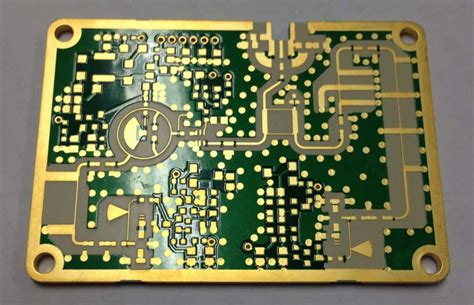
Key PCB Panelization Rules
To ensure successful panelization, designers must follow specific rules:
1. Panel Size Considerations
- Standard panel sizes vary by manufacturer (e.g., 18″ x 24″, 21″ x 24″).
- Avoid exceeding the manufacturer’s maximum panel size.
- Maintain a clearance of at least 5mm between PCBs and panel edges.
2. Spacing Between PCBs
- For V-scoring: Leave at least 0.5mm spacing.
- For tab routing: Ensure 2-3mm spacing for breakaway tabs.
- For perforated panels: Allow space for routing paths.
3. Fiducial Marks and Tooling Holes
- Add fiducial marks (at least 3 per panel) for automated assembly alignment.
- Include tooling holes (3-4mm diameter) for secure panel handling.
4. Tab Placement and Design
- Place tabs at least 5mm away from sensitive components.
- Use 3-5 tabs per side for stability.
- Tab width should be 2-3mm with 0.8-1mm mouse bites (if used).
5. Depanelization Method Selection
- Choose V-scoring for rectangular boards.
- Use tab routing for complex shapes.
- Avoid solid tabs if manual separation is needed.
6. Copper Balancing
- Ensure even copper distribution to prevent warping.
- Add copper thieving (dummy copper fills) if necessary.
7. Component Clearance
- Keep components at least 3mm away from panel edges.
- Avoid placing tall components near breakaway tabs.
8. Labeling and Orientation
- Mark PCB orientation (e.g., “TOP,” “BOTTOM”).
- Include panel numbers for traceability.
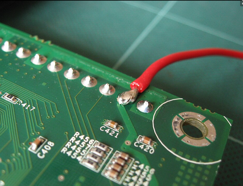
Best Practices for PCB Panelization
- Consult the Manufacturer Early – Discuss panelization requirements before finalizing the design.
- Minimize Waste – Optimize PCB arrangement to maximize panel utilization.
- Test Depanelization – Verify that boards can be separated without damage.
- Consider Assembly Needs – Ensure the panel can fit into pick-and-place machines.
- Avoid Mixed Materials in a Single Panel – Different PCB materials may require separate panels.
Conclusion
PCB panelization is a critical step in PCB manufacturing that enhances efficiency, reduces costs, and improves assembly reliability. By selecting the right panelization method (V-scoring, tab routing, perforated, or frameless) and following key design rules (spacing, fiducials, tab placement, and depanelization), designers can ensure smooth production and high-quality PCB assemblies. Always collaborate with manufacturers to optimize panel layouts and avoid costly errors.
By adhering to these guidelines, engineers can achieve cost-effective, high-yield PCB production while maintaining design integrity and manufacturability.