
Populated PCB: The Backbone of Modern Electronics
Introduction
Printed Circuit Boards (PCBs) are the foundation of virtually all modern electronic devices. From smartphones and computers to medical equipment and automotive systems, PCBs play a critical role in enabling the functionality of these devices. A populated PCB, also known as an assembled PCB, refers to a PCB that has been fully equipped with all the necessary electronic components, such as resistors, capacitors, integrated circuits (ICs), and connectors. This article delves into the intricacies of populated PCBs, exploring their design, manufacturing process, applications, and the challenges associated with their production.
1. The Anatomy of a Populated PCB
A populated PCB consists of two main elements: the bare PCB and the electronic components mounted on it.
1.1 Bare PCB
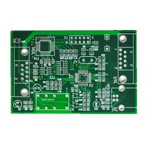
The bare PCB serves as the physical platform for the electronic components. It is typically made of a non-conductive substrate, such as fiberglass, coated with a thin layer of conductive material, usually copper. The copper layer is etched to create a network of pathways, known as traces, that connect the various components on the board. These traces form the electrical circuits that enable the device to function.
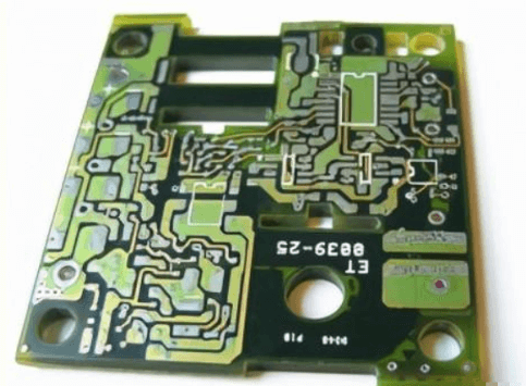
Bare PCBs can be single-sided, double-sided, or multi-layered, depending on the complexity of the device. Single-sided PCBs have conductive traces on only one side of the substrate, while double-sided PCBs have traces on both sides. Multi-layered PCBs, which are used in more complex devices, consist of multiple layers of conductive traces separated by insulating layers.
1.2 Electronic Components
The electronic components mounted on a PCB can be broadly categorized into two types: through-hole components and surface-mount components.
- Through-Hole Components: These components have leads that are inserted into holes drilled in the PCB and soldered to pads on the opposite side. Through-hole components are typically larger and more robust, making them suitable for applications that require high mechanical strength and reliability.
- Surface-Mount Components: These components are mounted directly onto the surface of the PCB. They are smaller and lighter than through-hole components, allowing for higher component density and more compact designs. Surface-mount technology (SMT) has become the dominant method for populating PCBs due to its efficiency and ability to support miniaturization.
2. The PCB Assembly Process
The process of populating a PCB involves several steps, each of which requires precision and attention to detail. The main stages of PCB assembly are as follows:
2.1 Solder Paste Application
The first step in the assembly process is the application of solder paste to the PCB. Solder paste is a mixture of tiny solder particles and flux, which helps the solder adhere to the components and the PCB. The solder paste is applied to the PCB using a stencil, which ensures that the paste is deposited only on the areas where components will be placed.
2.2 Component Placement
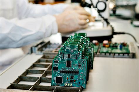
Once the solder paste has been applied, the next step is to place the electronic components onto the PCB. This is typically done using automated pick-and-place machines, which use robotic arms to accurately position the components on the board. The components are held in place by the tackiness of the solder paste.
2.3 Reflow Soldering
After the components have been placed, the PCB is passed through a reflow oven. The oven heats the PCB to a temperature that melts the solder paste, forming a permanent electrical and mechanical connection between the components and the PCB. The reflow process must be carefully controlled to ensure that the solder joints are strong and reliable.
2.4 Inspection and Testing
Once the soldering process is complete, the populated PCB undergoes inspection and testing to ensure that all components have been correctly placed and that there are no defects. Automated optical inspection (AOI) systems are commonly used to check for issues such as misaligned components, solder bridges, and insufficient solder. Functional testing may also be performed to verify that the PCB operates as intended.
2.5 Cleaning and Finishing
After inspection and testing, the PCB may be cleaned to remove any flux residue or other contaminants. Depending on the application, the PCB may also undergo additional finishing processes, such as conformal coating, to protect it from environmental factors such as moisture, dust, and temperature extremes.
3. Applications of Populated PCBs
Populated PCBs are used in a wide range of applications across various industries. Some of the most common applications include:
3.1 Consumer Electronics
Populated PCBs are at the heart of virtually all consumer electronic devices, including smartphones, tablets, laptops, and televisions. The demand for smaller, lighter, and more powerful devices has driven the development of advanced PCB assembly techniques, such as high-density interconnect (HDI) technology, which allows for the creation of highly compact and complex PCBs.
3.2 Automotive Electronics
Modern vehicles rely heavily on populated PCBs for a variety of functions, including engine control, infotainment systems, and advanced driver-assistance systems (ADAS). Automotive PCBs must be able to withstand harsh environmental conditions, such as extreme temperatures, vibration, and exposure to chemicals. As a result, they are often designed with robust materials and protective coatings.
3.3 Medical Devices
Populated PCBs are used in a wide range of medical devices, from diagnostic equipment to implantable devices. Medical PCBs must meet stringent regulatory requirements and be highly reliable, as failures can have serious consequences. They are often designed with features such as high-density interconnects and advanced thermal management to ensure optimal performance.
3.4 Industrial Equipment
In industrial settings, populated PCBs are used in control systems, automation equipment, and power supplies. Industrial PCBs must be able to operate reliably in challenging environments, such as high temperatures, humidity, and exposure to dust and chemicals. They are often designed with ruggedized components and protective coatings to ensure long-term reliability.
3.5 Aerospace and Defense
Populated PCBs are used in a variety of aerospace and defense applications, including avionics, communication systems, and radar. Aerospace and defense PCBs must meet rigorous standards for reliability and performance, as they are often used in mission-critical applications. They are typically designed with high-reliability components and advanced materials to withstand the extreme conditions encountered in aerospace environments.
4. Challenges in Populated PCB Manufacturing
The production of populated PCBs presents several challenges, particularly as electronic devices become more complex and miniaturized. Some of the key challenges include:
4.1 Miniaturization
As electronic devices continue to shrink in size, the demand for smaller and more densely populated PCBs has increased. This trend has led to the development of advanced assembly techniques, such as microvia technology and chip-scale packaging, which allow for the creation of highly compact PCBs. However, miniaturization also presents challenges in terms of component placement, soldering, and inspection, as even small defects can have a significant impact on the performance of the PCB.
4.2 Thermal Management
As electronic components become more powerful, managing heat dissipation has become a critical issue in PCB design. Excessive heat can lead to component failure and reduced reliability. To address this challenge, PCB designers must carefully consider factors such as component placement, thermal vias, and the use of heat sinks and thermal interface materials.
4.3 Signal Integrity
In high-speed electronic devices, maintaining signal integrity is essential to ensure reliable operation. Signal integrity issues, such as crosstalk, reflections, and electromagnetic interference (EMI), can degrade the performance of the PCB. To mitigate these issues, PCB designers must carefully design the layout of the traces, use appropriate materials, and implement shielding techniques.
4.4 Environmental and Regulatory Compliance
Populated PCBs must comply with a range of environmental and regulatory standards, particularly in industries such as automotive, medical, and aerospace. For example, the Restriction of Hazardous Substances (RoHS) directive restricts the use of certain hazardous materials in electronic products. Compliance with these standards requires careful selection of materials and components, as well as rigorous testing and documentation.
5. Future Trends in Populated PCB Technology
The field of populated PCB technology is constantly evolving, driven by the demand for more advanced and reliable electronic devices. Some of the key trends shaping the future of populated PCBs include:
5.1 Advanced Materials
The development of new materials, such as high-performance substrates and conductive inks, is enabling the creation of PCBs with improved thermal, electrical, and mechanical properties. These materials are particularly important for applications such as 5G communications, where high-frequency signals and thermal management are critical.
5.2 Flexible and Stretchable PCBs
Flexible and stretchable PCBs are gaining traction in applications such as wearable devices and medical implants. These PCBs are made from flexible materials, such as polyimide, that can bend and stretch without losing functionality. This flexibility allows for the creation of devices that can conform to the shape of the human body or other irregular surfaces.
5.3 3D Printing
3D printing technology is being explored as a potential method for manufacturing PCBs. 3D printing allows for the creation of complex, three-dimensional PCB structures that cannot be achieved with traditional manufacturing methods. This technology has the potential to revolutionize PCB design by enabling greater customization and reducing the time and cost of prototyping.
5.4 Internet of Things (IoT)
The proliferation of IoT devices is driving the demand for small, low-power PCBs that can support wireless connectivity and sensor integration. IoT PCBs must be designed with a focus on energy efficiency, as many IoT devices are battery-powered and must operate for extended periods without maintenance.
Conclusion
Populated PCBs are the backbone of modern electronics, enabling the functionality of a wide range of devices across various industries. The process of populating a PCB involves several critical steps, from solder paste application to inspection and testing, each of which requires precision and attention to detail. As electronic devices continue to evolve, the challenges associated with PCB assembly, such as miniaturization, thermal management, and signal integrity, are becoming increasingly complex. However, advancements in materials, manufacturing techniques, and design tools are helping to address these challenges and drive the development of more advanced and reliable PCBs. As we look to the future, trends such as flexible PCBs, 3D printing, and IoT are poised to further transform the field of populated PCB technology, paving the way for the next generation of electronic devices.