Power PCB Design: Essential Considerations and Best Practices
Introduction
Printed Circuit Boards (PCBs) are the backbone of modern electronics, and when it comes to power electronics, designing a robust and efficient Power PCB is critical. Power PCBs handle high currents, high voltages, and significant thermal loads, making their design more complex than standard PCBs. This article explores the key aspects of Power PCB design, including material selection, layout techniques, thermal management, and best practices to ensure reliability and performance.
1. Understanding Power PCB Design
Power PCBs are specifically designed to manage high-power applications such as:
- Switching power supplies
- Motor controllers
- Inverters and converters
- Battery management systems (BMS)
- High-power LED drivers
Unlike signal PCBs, which focus on high-speed data transmission, Power PCBs prioritize:
- High current handling
- Low resistance paths
- Effective heat dissipation
- Minimized electromagnetic interference (EMI)
2. Key Considerations in Power PCB Design
2.1 Material Selection
The choice of PCB substrate significantly impacts performance:
- FR-4: Common for low-power applications but may not be suitable for high temperatures.
- Metal Core PCBs (MCPCB): Use aluminum or copper bases for better thermal conductivity.
- High-Tg (Glass Transition Temperature) Materials: Essential for high-temperature environments.
- Ceramic Substrates: Used in high-frequency, high-power applications due to excellent thermal properties.
2.2 Copper Thickness and Trace Width
- Thicker copper layers (2oz to 6oz) reduce resistance and improve current handling.
- Wider traces minimize voltage drop and heat generation.
- Current carrying capacity must be calculated using tools like IPC-2152 standards.
2.3 Thermal Management
Power components generate significant heat, requiring:
- Thermal vias to transfer heat to inner or bottom layers.
- Heat sinks attached to high-power components.
- Proper component spacing to avoid localized overheating.
- Thermal relief pads for soldering while maintaining heat dissipation.
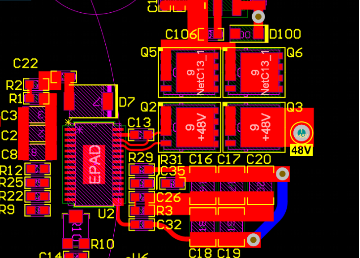
2.4 High-Current Routing Techniques
- Use of power planes instead of thin traces for high-current paths.
- Avoid sharp corners in traces to prevent current crowding.
- Kelvin connections for accurate voltage sensing in high-current applications.
2.5 EMI and Noise Reduction
- Proper grounding techniques (star grounding, ground planes).
- Shielding for sensitive components.
- Decoupling capacitors near power pins to filter noise.
- Minimizing loop areas to reduce inductive coupling.
3. Power PCB Layout Best Practices
3.1 Component Placement
- Power components (MOSFETs, diodes, inductors) should be placed close to minimize parasitic inductance.
- Thermal-sensitive components should be away from heat sources.
- Input and output filtering should be near connectors to reduce noise.
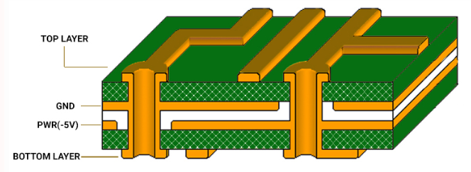
3.2 Layer Stackup Design
- Dedicated power and ground planes for low impedance paths.
- Signal layers sandwiched between ground planes for EMI reduction.
- Symmetrical stackup to prevent warping during manufacturing.
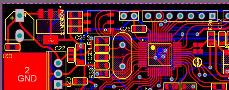
3.3 Via Usage
- Multiple vias in parallel reduce resistance and improve heat transfer.
- Avoid placing vias under high-power components to prevent solder wicking issues.
3.4 High-Voltage Considerations
- Creepage and clearance distances must comply with safety standards (IPC-2221, IEC 60950).
- Slotting or cutouts to increase isolation between high-voltage traces.
4. Simulation and Verification
Before manufacturing, simulation tools help validate the design:
- SPICE simulations for circuit behavior.
- Thermal analysis (e.g., Ansys, SolidWorks) to predict hotspots.
- Signal integrity checks for noise and EMI compliance.
4.1 Prototyping and Testing
- Measure voltage drops across high-current traces.
- Thermal imaging to identify overheating areas.
- EMI testing to ensure compliance with regulatory standards.
5. Common Power PCB Design Mistakes to Avoid
- Insufficient trace width leading to overheating.
- Poor thermal management causing component failure.
- Inadequate clearance leading to arcing in high-voltage designs.
- Improper grounding increasing noise and EMI.
- Ignoring manufacturing tolerances affecting reliability.
6. Future Trends in Power PCB Design
- Integration of wide-bandgap semiconductors (SiC, GaN) for higher efficiency.
- Advanced cooling techniques (embedded heat pipes, liquid cooling).
- 3D-printed PCBs for customized power electronics.
- AI-assisted PCB design for optimization and error reduction.
Conclusion
Designing a Power PCB requires careful consideration of material selection, thermal management, high-current routing, and EMI control. By following best practices in layout, simulation, and testing, engineers can develop reliable and efficient power electronics. As technology evolves, new materials and design methodologies will further enhance the performance of Power PCBs in high-demand applications.
By adhering to these principles, designers can ensure their Power PCBs meet performance, safety, and longevity requirements in today’s power-hungry electronic systems.