Power Plane Resonance Analysis in PCBs
Abstract
Power integrity (PI) is a critical aspect of modern high-speed printed circuit board (PCB) design. One of the key challenges in ensuring robust power delivery is mitigating power plane resonance, which can lead to noise, signal integrity issues, and electromagnetic interference (EMI). This paper explores the causes, analysis methods, and mitigation techniques for power plane resonance in PCBs. Through simulation and measurement approaches, designers can identify resonant frequencies and implement strategies to minimize their impact on system performance.

1. Introduction
As electronic systems operate at higher frequencies and lower voltages, maintaining power integrity becomes increasingly challenging. Power distribution networks (PDNs) in PCBs must provide stable voltage levels with minimal noise. However, power and ground planes in multilayer PCBs can act as resonant cavities, leading to standing waves at specific frequencies. These resonances can couple noise into signals, degrade power quality, and cause EMI.
This paper discusses:
- The physics of power plane resonance
- Analytical and simulation-based methods for resonance analysis
- Measurement techniques for identifying resonant frequencies
- Mitigation strategies to reduce resonance effects
2. Physics of Power Plane Resonance
Power and ground planes in a PCB form a parallel-plate waveguide structure. When excited by high-frequency signals (e.g., from switching ICs or signal transitions), electromagnetic waves propagate between the planes. At certain frequencies, these waves reflect off the plane edges, creating standing waves known as resonant modes.
2.1 Resonant Frequency Calculation
The resonant frequencies of a rectangular power plane can be approximated using the cavity resonator model:
[
f_{m,n} = \frac{c}{2\sqrt{\varepsilon_r}} \sqrt{\left( \frac{m}{L} \right)^2 + \left( \frac{n}{W} \right)^2}
]
Where:
- ( f_{m,n} ) = Resonant frequency for mode (m, n)
- ( c ) = Speed of light (~3×10⁸ m/s)
- ( \varepsilon_r ) = Relative permittivity of the dielectric material
- ( L, W ) = Length and width of the power plane
- ( m, n ) = Mode integers (0,1,2,…)
For example, a 10 cm × 8 cm FR-4 PCB plane (( \varepsilon_r \approx 4.3 )) has its first resonant mode (1,0) at:
[
f_{1,0} = \frac{3 \times 10^8}{2 \sqrt{4.3}} \left( \frac{1}{0.1} \right) \approx 720 \, \text{MHz}
]
Higher-order modes (e.g., (1,1), (2,0)) will occur at higher frequencies.
2.2 Impact of Resonance on Power Integrity
When the PDN is excited at a resonant frequency, the following issues may arise:
- Increased power supply noise due to standing waves
- Coupling into signal traces, causing jitter and distortion
- Radiated EMI from the PCB edges
- Reduced decoupling capacitor effectiveness at resonant frequencies
3. Analysis Methods for Power Plane Resonance
To predict and mitigate resonance, engineers use analytical models, simulations, and measurements.
3.1 Analytical Approaches
- Transmission Line Matrix (TLM) Methods: Model the power plane as a grid of transmission lines.
- Partial Element Equivalent Circuit (PEEC): Represents the plane as an RLC network.
- Cavity Model: Solves Maxwell’s equations for the plane boundaries.
3.2 Simulation Techniques
Modern PCB design tools use electromagnetic (EM) solvers to analyze resonance:
- Finite Element Method (FEM): Suitable for complex geometries.
- Method of Moments (MoM): Efficient for planar structures.
- 3D Full-Wave Solvers: Provide accurate results but require significant computation.
Example simulation steps in ANSYS HFSS or Keysight ADS:
- Define power/ground plane geometry and material properties.
- Apply ports to simulate noise injection.
- Perform frequency-domain analysis to extract impedance profiles.
- Identify peaks in the impedance plot (indicating resonances).
3.3 Measurement Techniques
- Vector Network Analyzer (VNA) Measurements: Measure PDN impedance vs. frequency.
- Near-Field Probes: Detect resonant emissions.
- Time-Domain Reflectometry (TDR): Identify impedance discontinuities.
4. Mitigation Strategies
Several techniques can reduce power plane resonance effects:
4.1 Decoupling Capacitors
- Place decoupling capacitors strategically to suppress resonances.
- Use a mix of bulk, ceramic, and high-frequency capacitors.
- Optimize capacitor placement using simulation.
4.2 Split Power Planes
- Divide large planes into smaller sections to shift resonant frequencies higher.
- Avoid splits under high-speed signal paths.
4.3 Stitching Vias and Damping
- Add stitching vias between power and ground planes to reduce cavity effects.
- Use resistive or ferrite materials to dampen resonances.
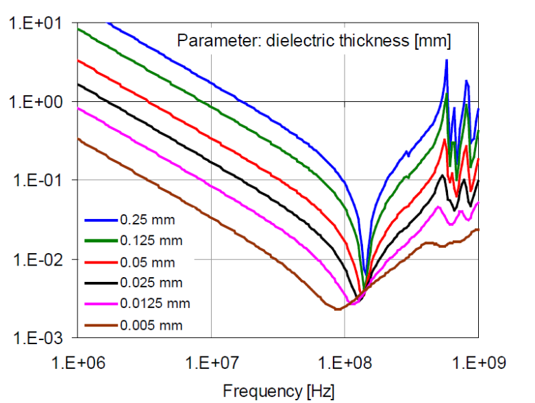
4.4 Embedded Capacitance
- Employ thin dielectric materials to increase interplane capacitance.
- Reduces high-frequency impedance.
4.5 Edge Termination
- Apply lossy materials or resistive terminations at plane edges to absorb reflections.
5. Case Study: Resonance Analysis in a High-Speed PCB
A 6-layer PCB with a 5V power plane (10 cm × 8 cm, FR-4) was analyzed using HFSS. The simulation revealed a strong resonance at 720 MHz (mode (1,0)), causing noise coupling into a 1 GHz clock signal. By adding decoupling capacitors (10 nF and 100 pF) and stitching vias, the resonance peak was reduced by 12 dB.
6. Conclusion
Power plane resonance is a critical issue in high-speed PCB design, leading to noise, signal integrity degradation, and EMI. Through analytical modeling, simulation, and measurements, engineers can identify resonant frequencies and implement mitigation strategies such as optimized decoupling, plane segmentation, and damping techniques. As PCBs continue to operate at higher frequencies, advanced resonance control methods will remain essential for robust power integrity.