Reducing Near-Field EMI in PCBs Using Operational Amplifiers
Abstract
This paper explores techniques for minimizing near-field electromagnetic interference (EMI) in printed circuit boards (PCBs) through proper implementation of operational amplifiers (op-amps). Near-field EMI presents significant challenges in modern electronic design, particularly in sensitive analog circuits and mixed-signal systems. By understanding op-amp characteristics, PCB layout strategies, and EMI reduction principles, designers can effectively mitigate near-field interference. This article covers fundamental concepts, practical design techniques, and advanced methods for optimizing op-amp circuits to reduce EMI emissions and susceptibility.
1. Introduction to Near-Field EMI in PCBs
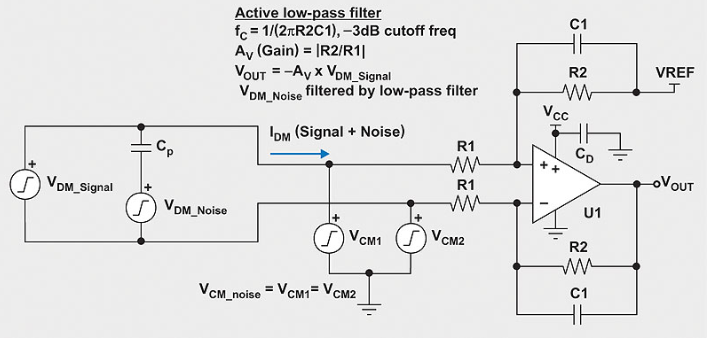
Electromagnetic interference exists in two primary forms: near-field and far-field. Near-field EMI, which occurs within a distance of λ/2π from the source (where λ is the wavelength), dominates in PCB environments where circuit elements are closely spaced. This interference can couple through either electric fields (capacitive coupling) or magnetic fields (inductive coupling), potentially degrading signal integrity and system performance.
Operational amplifiers, as fundamental building blocks in analog circuits, can both generate and be susceptible to near-field EMI. Their high gain and bandwidth make them particularly vulnerable to electromagnetic disturbances. However, when properly implemented, op-amps can also serve as tools for reducing overall system EMI.
2. Op-Amp Characteristics Affecting EMI Performance
2.1 Bandwidth and Slew Rate Considerations
The bandwidth and slew rate of an op-amp directly influence its EMI characteristics. High-bandwidth amplifiers tend to amplify higher frequency noise, while devices with fast slew rates can generate high-frequency harmonics. Selecting an op-amp with appropriate specifications for the application helps minimize unnecessary high-frequency content that contributes to near-field EMI.
2.2 Power Supply Rejection Ratio (PSRR)
A high PSRR enables the op-amp to reject power supply noise, preventing it from appearing at the output where it could radiate or couple to nearby circuits. Modern precision op-amps often feature PSRR values exceeding 100 dB at DC, though this typically decreases with frequency.
2.3 Common-Mode Rejection Ratio (CMRR)
CMRR measures an op-amp’s ability to reject interference that appears equally on both inputs. High CMRR is particularly valuable in reducing susceptibility to common-mode near-field EMI.
2.4 Output Impedance and Drive Capability
The output characteristics of an op-amp affect its ability to drive capacitive loads without ringing or oscillation, which are significant sources of high-frequency EMI.
3. PCB Layout Techniques for EMI Reduction
3.1 Proper Grounding Strategies
- Implement a solid ground plane to provide low-impedance return paths
- Use star grounding for sensitive analog sections
- Avoid ground loops that can act as antennas for EMI
- Separate analog and digital grounds properly, with single-point connection if necessary
3.2 Power Supply Decoupling
- Place decoupling capacitors as close as possible to op-amp power pins
- Use multiple capacitor values in parallel to cover different frequency ranges
- Consider ferrite beads in series with power lines for additional high-frequency filtering
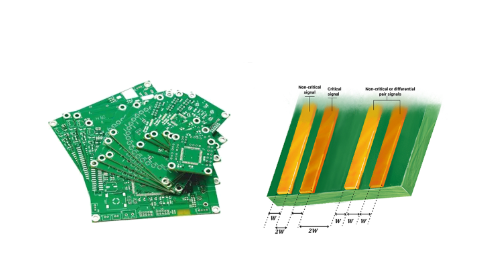
3.3 Signal Routing Best Practices
- Keep high-impedance nodes as short as possible to reduce capacitive pickup
- Route sensitive traces away from potential interference sources
- Use differential signaling where applicable to improve common-mode rejection
- Implement proper transmission line techniques for high-frequency signals
3.4 Component Placement
- Position op-amps away from known EMI sources (switching regulators, clock circuits)
- Orient components to minimize loop areas in critical current paths
- Group related components functionally to minimize interconnect lengths
4. Advanced Techniques for EMI Reduction
4.1 Filtering and Compensation
- Add low-pass filtering at op-amp inputs and outputs where appropriate
- Use feedforward compensation techniques to reduce high-frequency gain
- Implement EMI filters specifically designed for the expected interference spectrum
4.2 Shielding Methods
- Apply localized shielding for particularly sensitive circuits
- Use guard rings around high-impedance inputs
- Consider board-level shielding cans in extreme cases
4.3 Differential Amplifier Configurations
Differential amplifier topologies inherently reject common-mode interference when properly balanced. Key considerations include:
- Precise matching of resistor networks
- Symmetrical layout of differential pairs
- Common-mode feedback techniques for improved performance
4.4 Current Feedback Amplifier Advantages
Current feedback amplifiers (CFAs) offer potential EMI benefits in some applications:
- More stable input impedance over frequency
- Potentially better large-signal bandwidth characteristics
- Different noise susceptibility profile compared to voltage feedback amplifiers
5. Measurement and Verification Techniques
5.1 Near-Field Probing
- Use H-field and E-field probes to identify EMI hotspots
- Perform scans at various frequencies of interest
- Compare measurements before and after implementing improvements
5.2 Frequency Domain Analysis
- Conduct FFT analysis of op-amp outputs to identify unintended spectral content
- Measure power supply noise and its coupling into signals
- Analyze harmonic distortion products that may indicate nonlinear behavior
5.3 Time Domain Reflectometry
- Identify impedance mismatches that could cause reflections and ringing
- Verify proper termination of transmission lines
- Characterize discontinuities in the signal path
6. Case Studies and Practical Examples
6.1 Reducing EMI in Precision Measurement Circuits
A case study demonstrating how proper op-amp selection and layout reduced near-field EMI by 18 dB in a sensitive weighing scale application.
6.2 Audio Application EMI Reduction
Implementation of EMI-reduction techniques in a professional audio mixer, focusing on op-amp power supply conditioning and input protection networks.
6.3 Medical Instrumentation Example
How medical device designers achieved FDA EMI compliance through careful op-amp circuit implementation and PCB layout optimization.
7. Future Trends and Developments
Emerging technologies that may further improve op-amp EMI performance:
- Integrated EMI filters within op-amp packages
- Advanced packaging techniques for better shielding
- Adaptive compensation circuits that respond to detected interference
- Machine learning-assisted PCB layout optimization for EMI reduction
8. Conclusion
Effective reduction of near-field EMI in PCBs using operational amplifiers requires a holistic approach combining proper device selection, circuit design techniques, and meticulous PCB layout practices. By understanding the mechanisms of EMI generation and coupling in op-amp circuits, designers can implement strategies that significantly improve electromagnetic compatibility without compromising circuit performance. The techniques discussed in this paper provide a foundation for addressing near-field EMI challenges across a wide range of applications, from consumer electronics to critical medical and industrial systems.
As electronic systems continue to increase in complexity and density, the importance of EMI-conscious design grows correspondingly. Operational amplifiers, when properly implemented, can serve as both workhorses of analog signal processing and allies in the battle against electromagnetic interference.