RF and Mixed-Signal High-Speed PCB Design: Challenges and Best Practices
Abstract
The increasing demand for high-performance electronic systems has led to the widespread adoption of radio frequency (RF) and mixed-signal (analog/digital) high-speed PCB designs. These designs are critical in applications such as 5G communications, IoT devices, automotive radar, and high-speed data acquisition systems. However, integrating RF and high-speed digital signals on the same PCB introduces significant challenges, including signal integrity (SI), power integrity (PI), electromagnetic interference (EMI), and crosstalk. This article explores the key considerations, design techniques, and best practices for successful RF and mixed-signal high-speed PCB design.
1. Introduction
Modern electronic systems often require the integration of RF circuits (operating at GHz frequencies) alongside high-speed digital and analog components. The coexistence of these signals on a single PCB introduces complex design challenges due to differing signal behaviors, noise sensitivity, and interference mechanisms. Effective PCB design must address impedance matching, grounding strategies, noise suppression, and thermal management to ensure optimal performance.
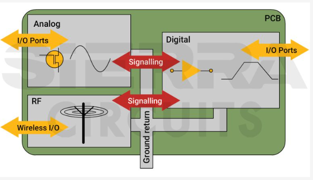
2. Key Challenges in RF and Mixed-Signal PCB Design
2.1 Signal Integrity (SI) Issues
- Impedance Mismatch: RF signals require controlled impedance traces (typically 50Ω for RF, 100Ω for differential pairs) to minimize reflections.
- Skin Effect & Dielectric Losses: At high frequencies, current flows near the conductor surface, increasing resistance and signal attenuation.
- Crosstalk: High-speed digital signals can couple into sensitive RF traces, degrading signal quality.
2.2 Power Integrity (PI) Considerations
- Voltage Ripple & Noise: High-speed digital circuits generate switching noise that can disrupt RF and analog circuits.
- Decoupling Strategies: Proper use of decoupling capacitors and power plane segmentation is essential to minimize noise.
2.3 Electromagnetic Interference (EMI)
- Radiated Emissions: High-frequency signals can radiate EMI, affecting nearby circuits and violating regulatory standards.
- Grounding & Shielding: Proper grounding techniques and shielding structures (e.g., Faraday cages) are necessary to contain EMI.
2.4 Thermal Management
- Heat Dissipation: RF power amplifiers and high-speed processors generate significant heat, requiring thermal vias and heatsinks.
3. Best Practices for RF and Mixed-Signal PCB Design
3.1 Stackup Design
- Controlled Dielectric Layers: Use high-frequency laminates (e.g., Rogers, Isola) for RF sections to minimize losses.
- Separate Ground Planes: Isolate analog, digital, and RF ground planes to prevent noise coupling.
- Power Plane Segmentation: Dedicate separate power planes for RF, analog, and digital sections.
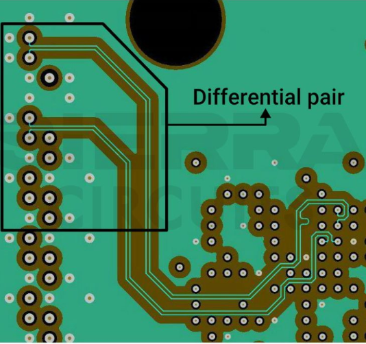
3.2 Routing Strategies
- Minimize Trace Lengths: Keep RF traces as short as possible to reduce losses.
- Avoid Right-Angle Bends: Use 45° or curved traces to prevent impedance discontinuities.
- Differential Pair Routing: Maintain consistent spacing and length matching for differential signals.
3.3 Grounding Techniques
- Star Grounding: Connect all ground returns to a single point to avoid ground loops.
- Split Ground Planes: Use moats or slots to isolate noisy digital grounds from sensitive analog/RF grounds.
- Via Shielding: Place ground vias around RF traces to reduce interference.
3.4 EMI Mitigation
- Shielding Cans: Enclose RF circuits in metal shields to block external noise.
- Ferrite Beads & Filters: Use filtering components to suppress high-frequency noise.
- Proper Return Paths: Ensure uninterrupted return paths for high-speed signals.
3.5 Simulation & Validation
- EM Simulation Tools: Use tools like Ansys HFSS, Keysight ADS, or Cadence Sigrity for SI/PI/EMI analysis.
- Time-Domain Reflectometry (TDR): Verify impedance matching and trace integrity.
- Network Analyzer Testing: Measure S-parameters to validate RF performance.
4. Case Study: 5G mmWave PCB Design
A 5G mmWave (28GHz) PCB design requires:
- Low-Loss Materials: PTFE-based substrates for minimal dielectric loss.
- Antenna Integration: Microstrip or patch antennas with impedance matching networks.
- High-Speed Digital Interfaces: PCIe, DDR4 routing with strict length matching.
5. Conclusion
Designing RF and mixed-signal high-speed PCBs requires a multidisciplinary approach, balancing signal integrity, power integrity, and EMI control. By following best practices in stackup design, routing, grounding, and simulation, engineers can achieve robust and high-performance PCB layouts. As technology advances toward higher frequencies (6G, terahertz), these design principles will become even more critical