
Skip to content
Andwin Circuits
  • Home
  • ProductsExpand
    • HDI multilayer PCB
    • Rigid Flex PCB
    • Flex pcb
    • Special PCBExpand
      • High Frequency PCBExpand
        • Rogers RO4350B PCB
        • Rogers RO4003 pcb
        • Rogers RO3003 PCB
        • Rogers 5880 PCB
        • DICLAD 527 PCB
        • Taconic TLX series
        • Taconic TLX-8 RF PCB
        • Taconic TLX-9 RF PCB
      • High speed pcbExpand
        • Megtron 6 High Speed PCB
        • TU-872 SLK Sp High Speed
      • High TG PCBExpand
        • SHENGYI SH260 PCB
        • ISOLA 370HR PCB
        • ISOLA IS410 PCB
        • ISOLA IS420 PCB
      • Heavy copper PCB
      • Copper coin pcb
      • Copper inlay PCB
    • Metal Core PCBExpand
      • Copper core pcb
      • Aluminum PCB
      • 2 Layers Aluminum PCB
      • Direct thermal MCPCB
      • 2 Layers Direct Thermal
    • Ceramic PCBExpand
      • DPC ceramic PCB
      • DBC ceramic PCB
      • Thick film Ceramic PCB
      • Al2O3 Alumina PCB
      • AIN ALN ceramic PCB
      • IGBT Ceramic PCB
  • ServiceExpand
    • PCB Assembly
    • Quick turn PCB assembly
    • PCBA conformal coating
  • IndustryExpand
    • Telecommunication
    • IoT and Wireless
    • Industrial Control
    • Thermal management
    • Power and Energy
    • IC test board
    • Automative
    • Medical
  • CapabilityExpand
    • Rigid PCB
    • Rigid flex PCB
    • Metal core PCB
    • PCB Assembly
  • TechnologyExpand
    • Blogs
    • Via in pad
    • PCB E-test
    • PCB stack up
    • MCPCB panelization
    • Controlled impedance PCB
  • AboutExpand
    • About us
    • Certification
    • Factory Tour
  • Contact
Andwin Circuits
Home / RF Layout Guidelines for Mobile Phone PCB Design

RF Layout Guidelines for Mobile Phone PCB Design

ByGrace June 7, 2025June 5, 2025

Introduction

The design of Radio Frequency (RF) circuits in mobile phone Printed Circuit Boards (PCBs) is critical to ensuring optimal performance, signal integrity, and minimal interference. With the increasing complexity of modern smartphones—supporting multiple wireless standards such as 5G, Wi-Fi 6, Bluetooth, and GNSS—proper RF PCB layout has become more challenging yet essential.

This article discusses key considerations and best practices for RF layout in mobile phone PCB design, covering component placement, grounding, impedance control, shielding, and interference mitigation.

1. Understanding RF PCB Design Challenges

RF circuits operate at high frequencies, making them highly sensitive to noise, crosstalk, and impedance mismatches. Poor RF layout can lead to:

  • Signal degradation (attenuation, reflection, distortion)
  • Increased electromagnetic interference (EMI)
  • Reduced wireless range and data throughput
  • Higher power consumption

To avoid these issues, designers must follow RF-specific layout principles while balancing space constraints in compact mobile devices.
Contact us for PCB quote now |

2. Key RF Layout Considerations

2.1. Component Placement

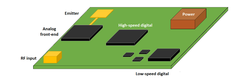
  • Isolate RF sections: Keep RF components (PA, LNA, filters, antennas) away from noisy digital circuits (processors, memory, power supplies).
  • Minimize trace lengths: Place RF components as close as possible to reduce parasitic inductance/capacitance.
  • Antenna positioning: Antennas should be placed at the edge of the PCB, away from metal components and ground planes that could detune them.

2.2. Grounding and Power Distribution

  • Use a solid ground plane: A continuous ground plane beneath RF traces reduces loop inductance and EMI.
  • Separate RF and digital grounds: Use a single-point connection or ferrite bead to prevent ground noise coupling.
  • Decoupling capacitors: Place them near RF ICs to filter high-frequency noise.

2.3. Impedance Control and Transmission Lines

  • Match trace impedance: Use controlled impedance traces (typically 50Ω for RF lines) with proper width and dielectric spacing.
  • Avoid sharp bends: Use 45° or curved traces to prevent impedance discontinuities.
  • Microstrip vs. stripline:
  • Microstrip (top/bottom layer) is easier to tune but more susceptible to interference.
  • Stripline (inner layer) offers better shielding but is harder to modify.

2.4. Shielding and EMI Mitigation

  • RF shielding cans: Use metal shields over critical RF sections to block interference.
  • Via stitching: Place ground vias around RF traces to contain electromagnetic fields.
  • Keep-out zones: Prevent copper pours or components under antenna areas.

2.5. Crosstalk Prevention

  • Increase spacing: Maintain at least 3x the trace width between RF and high-speed digital lines.
  • Orthogonal routing: Run RF and digital traces perpendicular to each other to minimize coupling.
Contact us for PCB quote now |

3. Practical RF Layout Techniques

3.1. Layer Stackup Optimization

A typical 6-8 layer mobile PCB stackup may include:

  • Top Layer: RF components, antennas
  • Layer 2: Ground plane (critical for RF return path)
  • Layer 3-5: Signal and power layers
  • Bottom Layer: Additional RF or low-frequency circuits

3.2. Antenna Feedline Design

  • Use a pi-matching network to optimize antenna impedance.
  • Ensure minimal loss in the feedline by avoiding vias and using thick traces.

3.3. Testing and Validation

  • Perform S-parameter analysis to check signal integrity.
  • Use network analyzers to verify impedance matching.
  • Conduct EMI/EMC testing to ensure compliance with regulatory standards.

4. Common Mistakes to Avoid

❌ Ignoring return current paths: Poor grounding leads to noise coupling.
❌ Overlooking parasitic effects: Even small capacitances/inductances can degrade RF performance.
❌ Insufficient isolation: RF and digital circuits must be physically separated.
❌ Neglecting thermal management: RF power amplifiers generate heat, requiring proper thermal relief.

5. Conclusion

Designing an efficient RF layout for mobile phone PCBs requires careful planning, adherence to high-frequency principles, and iterative testing. By following best practices in component placement, grounding, impedance control, and shielding, designers can achieve optimal RF performance while minimizing interference in compact smartphone designs.

As wireless technologies evolve, RF PCB layout will continue to be a critical factor in ensuring reliable connectivity, making these guidelines indispensable for modern mobile device engineering.

Contact us for PCB quote now |

Post Tags: #aluminum clad pcb#aluminum core pcb#aluminum core pcb led#aluminum pcb#Mobile Phone PCB Design

Post navigation

Previous Previous
What is PCB Drilling Backer Board?
NextContinue
Why Design Balanced Stackup PCBs? What Are the Advantages?

Search

Search

Products

  • HDI Multilayer PCB
  • Rigid Flex PCB
  • Flex pcb
  • High Frequency PCB
  • High speed pcb
  • Heavy copper PCB
  • Metal Core PCB
  • Ceramic PCB

Address

Andwin Circuits Co.,Limited
Email: sales@andwinpcb.com
Tel: +86 755 2832 9394
Fax:+86 755 2992  6717
ADD:1-2F-1217,HouDeQun Industrial park,
NanTing RD NO.56,ShaJing,BaoAn,Shenzhen 518104,GuangDong,China

Products

  • HDI Multilayer PCB
  • Rigid Flex PCB
  • Flex pcb
  • High Frequency PCB
  • High speed pcb
  • Heavy copper PCB
  • Metal Core PCB
  • Ceramic PCB

Technology

  • Blogs
  • Via in pad
  • PCB E-test
  • PCB stack up
  • Metal core PCB panelization
  • Controlled impedance PCB

CERTIFICATION

Certification >>


Copyright© 2003 - 2026 Andwin | All Rights Reserved | Powered by Andwin

Scroll to top
  • Home
  • Products
    • HDI multilayer PCB
    • Rigid Flex PCB
    • Flex pcb
    • Special PCB
      • High Frequency PCB
        • Rogers RO4350B PCB
        • Rogers RO4003 pcb
        • Rogers RO3003 PCB
        • Rogers 5880 PCB
        • DICLAD 527 PCB
        • Taconic TLX series
        • Taconic TLX-8 RF PCB
        • Taconic TLX-9 RF PCB
      • High speed pcb
        • Megtron 6 High Speed PCB
        • TU-872 SLK Sp High Speed
      • High TG PCB
        • SHENGYI SH260 PCB
        • ISOLA 370HR PCB
        • ISOLA IS410 PCB
        • ISOLA IS420 PCB
      • Heavy copper PCB
      • Copper coin pcb
      • Copper inlay PCB
    • Metal Core PCB
      • Copper core pcb
      • Aluminum PCB
      • 2 Layers Aluminum PCB
      • Direct thermal MCPCB
      • 2 Layers Direct Thermal
    • Ceramic PCB
      • DPC ceramic PCB
      • DBC ceramic PCB
      • Thick film Ceramic PCB
      • Al2O3 Alumina PCB
      • AIN ALN ceramic PCB
      • IGBT Ceramic PCB
  • Service
    • PCB Assembly
    • Quick turn PCB assembly
    • PCBA conformal coating
  • Industry
    • Telecommunication
    • IoT and Wireless
    • Industrial Control
    • Thermal management
    • Power and Energy
    • IC test board
    • Automative
    • Medical
  • Capability
    • Rigid PCB
    • Rigid flex PCB
    • Metal core PCB
    • PCB Assembly
  • Technology
    • Blogs
    • Via in pad
    • PCB E-test
    • PCB stack up
    • MCPCB panelization
    • Controlled impedance PCB
  • About
    • About us
    • Certification
    • Factory Tour
  • Contact
Search