Setting and using the origin in Kicad PCB
KiCad can use three types of origins in the PCB editor: page origin, drilling/placement file origin, and grid origin. You can also customize the direction of the coordinate axis. ”
Introduction
KiCad is a CAD system based on 2D data, which requires coordinates to mark the position of objects. In theory, it is possible to rely entirely on constraints rather than coordinates in a CAD system, but KiCad cannot do that. There must be an internal coordinate system, and all well-defined positions must conform to this system.
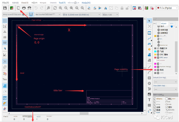
The PCB editor has a precision of 1 nanometer, which is the smallest difference that two positions can have in the X or Y direction. It has an internal (0,0) coordinate system origin, which is the “page origin” – the upper left corner of the page area you see when you open Pcbnew. In the internal coordinate system, X increases from left to right, which is normal, but Y increases from top to bottom, which is different from commonly used CAD (such as AD). This is due to historical reasons. The opposite Y axis coordinate is very annoying for some users, but fortunately it can now be modified through configuration.
Configure origin and coordinate direction
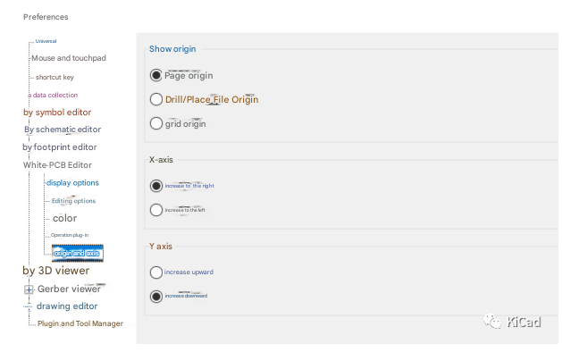
Starting from KiCad 6, you can configure both the visible origin and the coordinate axis direction. You can configure it in “Preferences -> PCB Editor -> Origin and Axes page. There are three choices for displaying the origin:
Page Origin (default)
Drill/Placement File Origin
Grid Origin
While it is logically possible to set different origins and coordinate axis directions, we must be aware that these only change the visible coordinates in the GUI. The internal coordinate system and board files are not affected. Also note that the origin of the drill/placement file may change the output of the footprint placement file and drill file.
Different Origins
Page Origin
This is the same as the internal origin of Pcbnew’s coordinate system. Pcbnew has a The concept of a “page”, although the main purpose of page layout is not printing.
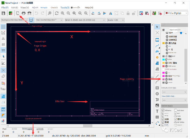
By default, the page origin is used as the origin of the visible coordinates. Internal X coordinate values increase from left to right, and Y coordinate values increase from top to bottom. The page origin cannot be changed.
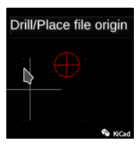
Drill/place file origin
This is also called the “auxiliary origin”.
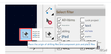
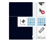
This is a point that can be set by the user. Earlier (in v5 and before) it was possible to use it as the origin when exporting certain files, and now it can also be used as the origin of the visual coordinates. Select “Place->Drill/Place File Origin” or use the toolbar on the right to place the origin.
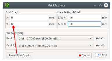
Grid Origin
KiCad uses the concept of grid to solve the problem of 1 nanometer accuracy that cannot be used directly. A user-defined grid is valid at all times. When objects are placed or moved, the cursor is usually attached to the grid grid points, but will not exceed the grid grid points. For example, commonly used grid accuracy can be 0.1mm or 10mil.
If the user always keeps the same fine-pitch grid, the concept of independent grid origin is not necessarily needed. Suppose a 10x10mm grid is used, and an object is placed at each grid point. By default, the grid starts from the internal 0,0 origin, so there are some grid points at: such as (100,100), (110,100), (120,100).
However, if you start at (101,101) but still use the desired 10x10mm grid, a movable grid origin becomes useful. By opening View->Grid Properties, you can set the grid points that define the grid.

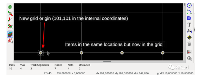
A serious problem can occur when changing the grid origin. As can be seen in the illustration above, objects that were positioned using the old grid origin will fall off the grid after the origin is changed, and vice versa. If a PCB has already been designed with a certain grid, and then the origin is changed for some reason, it should be returned to the original origin, otherwise problems will arise because most objects will now be off the grid.
Using “Placement” -> “Grid Origin”, or use the toolbar on the right hand side to change the grid origin.
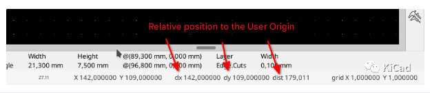
User Origin and Coordinates
KiCad has a very convenient way to measure and view the position of an object relative to a coordinate point without changing the coordinate system. Just press the space bar on the keyboard, it sets the “local origin” (sometimes called the “user origin”). It is a temporary point, intended as a quick helper, not a permanent reference point. It is very useful when measuring distances and placing objects.